 ChipApex | Global Electronic Components Supplier

SEARCH
Search Product
Search Post
— IC芯片 | 连接器 | 传感器 | 被动器件 —
Search productSearch post
— IC芯片 | 连接器 | 传感器 | 被动器件 —
Consult the customer manager about the wholesale price.
consultation hotline:86-132-6715-2157
email:[email protected]
Contact the product manager for consultation. One-stop consultation is available.
Do you want a lower wholesale price? Please send us your inquiry and we will reply immediately.
The AD7248AANZ is a monolithic 12-bit voltage output digital-to-analog converter featuring an integrated output amplifier and buried Zener reference. It utilizes LC2MOS technology for precision bipolar circuits combined with low-power CMOS logic. The device accepts 12-bit data via an 8-bit parallel bus loaded in two write operations, controlled by CSMSB, CSLSB, and WR signals. An asynchronous LDAC signal updates the analog output. It operates from single or dual supplies (+12 V to +15 V) and supports output ranges of 0–5 V, 0–10 V, or ±5 V. Key specifications include ±1/2 LSB relative accuracy, 30 ns typical data setup time, and 65 mW typical power dissipation in single-supply mode.
Verify the ordering suffix 'ANZ' corresponds to the Plastic DIP-20 package with RoHS compliance as per the manufacturer's current catalog. Confirm the temperature range is –40 °C to +85 °C. Ensure the specific linearity grade matches system requirements, as the 'A' suffix denotes ±3/4 LSB while 'B' denotes ±1/2 LSB.
Select the AD7248A over the AD7245A when interfacing with microprocessors having an 8-bit wide data bus, as it requires two write cycles for full 12-bit loading. Choose the 'A' version for standard commercial applications requiring ±3/4 LSB accuracy, or the 'B' version for higher precision needs at ±1/2 LSB. Ensure supply voltages remain within +12 V to +15 V for specified performance.
The AD7248A is part of the enhanced AD7245A/AD7248A family, improving upon the legacy AD7245/AD7248 models. It offers faster interface times, extended temperature ranges, and better full-scale variation with supply voltage changes. The AD7248A variant specifically targets systems using 8-bit data buses, whereas the AD7245A supports direct 12-bit parallel loading.
The AD7248ABN is a pin-compatible alternative with improved ±1/2 LSB linearity accuracy. For military specifications, the AD7248ATQ processed to MIL-STD-883 Class B is available. Direct replacement with non-enhanced AD7248 parts may require verification of interface timing and supply voltage compatibility.
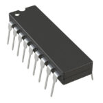 AD7248AANZ

The activity of extra discounts on wholesale prices is in full swing…
Please fill in your contact information and we will send you the latest wholesale price list.





