 ChipApex | Global Electronic Components Supplier
SEARCH
Search Product
Search Post
— IC芯片 | 连接器 | 传感器 | 被动器件 —
Search productSearch post
— IC芯片 | 连接器 | 传感器 | 被动器件 —
Consult the customer manager about the wholesale price.
consultation hotline:86-132-6715-2157
email:[email protected]
Contact the product manager for consultation. One-stop consultation is available.
Do you want a lower wholesale price? Please send us your inquiry and we will reply immediately.
The AD75019JPZ-REEL is a 16 × 16 crosspoint switch array containing 256 analog switches in a compact 44-lead PLCC package. It accommodates signal ranges up to supply rails of ±12 V or 24 V, with a typical on-resistance of 150 Ω at ±12 V and 300 Ω at ±5 V. The device features TTL/CMOS-compatible control lines and utilizes a serial input interface for simplified programming. Data is loaded via a dynamic 256-bit shift register clocked by SCLK (20 kHz min to 5 MHz max) and transferred to static latches via PCLK. Quiescent power consumption is low at 2 mW. The component supports cascading through a serial output pin.
Verify the specific ordering suffix matches the required packaging format. Confirm that the RoHS compliant status aligns with environmental regulations for the target assembly process. Ensure the operating temperature range meets the application's thermal requirements before finalizing procurement orders.
Select this component when a high-density crosspoint switching solution is required with minimal control wiring. Consider the on-resistance specifications relative to the intended signal voltage levels. Verify that the available clock frequencies meet the system's data loading speed requirements and that the power supply sequencing constraints can be satisfied within the design.
This part belongs to the Analog Devices AD75019 family of crosspoint switch arrays. It is fabricated using BiMOS II technology, which integrates CMOS devices for low distortion switching and bipolar devices for ESD protection. The device is designed for applications requiring flexible interconnection between multiple input and output lines.
The AD75019JPZ is the non-reel version of this component. No other direct substitute part numbers are documented in the official datasheet.
The serial shift register is dynamic and requires a minimum clock rate of 20 kHz to prevent data loss.
VDD must always be greater than (VCC – 0.5 V), and VSS must always be less than (DGND + 0.5 V). External diodes may be used if proper sequencing cannot be ensured.
Yes, multiple devices can be cascaded by connecting the SOUT output of one device to the SIN input of the next.
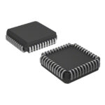 AD75019JPZ-REEL
The activity of extra discounts on wholesale prices is in full swing…
Please fill in your contact information and we will send you the latest wholesale price list.





