 ChipApex | Global Electronic Components Supplier
SEARCH
Search Product
Search Post
— IC芯片 | 连接器 | 传感器 | 被动器件 —
Search productSearch post
— IC芯片 | 连接器 | 传感器 | 被动器件 —
Consult the customer manager about the wholesale price.
consultation hotline:86-132-6715-2157
email:[email protected]
Contact the product manager for consultation. One-stop consultation is available.
Do you want a lower wholesale price? Please send us your inquiry and we will reply immediately.
The AD7740YRMZ is a low-cost, ultrasmall synchronous Voltage-to-Frequency Converter (VFC) from Analog Devices. It operates on a single supply of 3.0 V to 3.6 V or 4.75 V to 5.25 V, consuming typically 0.9 mA. The device features an internal 2.5 V bandgap reference and accepts analog inputs from 0 V to VREF, with true capability down to -150 mV without a charge pump. The full-scale output frequency is set by the external clock on the CLKIN pin, ranging up to 1 MHz. Integral Nonlinearity is specified at ±0.012% of span in unbuffered mode. It is housed in an 8-lead MSOP package and guaranteed for automotive temperature ranges of -40°C to +105°C.
Verify that the specific part number suffix corresponds to the required operating temperature grade, as the Y designation indicates the automotive range of -40°C to +105°C. Confirm the package type matches the design footprint, specifically the 8-lead MSOP configuration. Ensure the power supply rails align with the specified 3.0 V to 3.6 V or 4.75 V to 5.25 V operational limits to maintain performance specifications.
Select this component when space constraints require an ultrasmall package solution for voltage-to-frequency conversion. It is suitable for designs needing ratiometric operation using the internal 2.5 V reference or external overdrive. Consider the buffered versus unbuffered input modes based on source impedance requirements and whether negative input voltages relative to ground are necessary for the application signal range.
This device belongs to the AD7740 family of synchronous voltage-to-frequency converters manufactured by Analog Devices. The family includes variants such as the K version for commercial temperatures and different packaging options like SOT-23. The AD7740 utilizes CMOS technology and charge-balance conversion techniques to achieve its performance characteristics within a compact form factor designed for cost-sensitive applications.
The AD7740KRMZ serves as a commercial grade alternative within the same package. Other members of the AD7740 series may offer different temperature ratings or package styles but share the core functional architecture.
The output frequency is synchronous with the clock signal on the CLKIN pin, which can be provided by an external CMOS-compatible clock source or generated by an external crystal connected between CLKIN and CLKOUT.
The BUF pin selects the input mode. When tied high, it enables a high impedance buffered mode with an input range of 0.1 V to VDD – 0.2 V. When tied low, it enables an unbuffered mode allowing inputs from -0.15 V to VDD + 0.15 V.
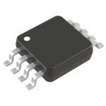 AD7740YRMZ
The activity of extra discounts on wholesale prices is in full swing…
Please fill in your contact information and we will send you the latest wholesale price list.





