 ChipApex | Global Electronic Components Supplier
AD7801BRU
Search Product
Search Post
— IC芯片 | 连接器 | 传感器 | 被动器件 —
Search productSearch post
— IC芯片 | 连接器 | 传感器 | 被动器件 —
Consult the customer manager about the wholesale price.
consultation hotline:86-132-6715-2157
email:[email protected]
Contact the product manager for consultation. One-stop consultation is available.
Do you want a lower wholesale price? Please send us your inquiry and we will reply immediately.
The AD7801BRU is an 8-bit voltage-output digital-to-analog converter (DAC) from Analog Devices Inc., housed in a 20-lead TSSOP package. It operates on a single supply ranging from +2.7 V to +5.5 V and features an internal precision output buffer capable of rail-to-rail swing. The device utilizes a parallel microprocessor-compatible interface with double-buffered logic for synchronous or automatic updates. Key electrical specifications include a maximum settling time of 2 µs, ±1 LSB relative accuracy, and ±1 LSB differential nonlinearity. Power consumption is typically 5 mW at 3.3 V, reducing to less than 3 µW in power-down mode.
Verify the specific suffix 'RU' corresponds to the 20-lead Thin Shrink Small Outline package as defined in the ordering guide. Confirm the temperature range matches the B version specification (-40 °C to +105 °C). Ensure compatibility with the required supply voltage range of 2.7 V to 5.5 V for the target application environment.
Select this component when an 8-bit resolution with rail-to-rail output is required in a compact surface-mount package. The internal reference simplifies design by eliminating external reference components if tied to VDD. Consider the 2 µs settling time and parallel interface speed for system timing constraints. Verify that the load requirements (10 kΩ to VDD/GND and 100 pF) are within the output buffer's drive capabilities.
The AD7801BRU is part of the AD7801 family, which includes variants in SOIC and TSSOP packages. The 'B' designation indicates the industrial temperature range (-40 °C to +105 °C), while 'RU' specifies the 20-lead TSSOP package option. This model is designed for applications requiring low power and simple parallel interfacing.
Publicly confirmed substitute part numbers are not available in the provided documentation. Users should consult official Analog Devices resources for cross-reference information.
The internal reference is selected by tying the REFIN pin directly to VDD. The internal circuitry detects this connection and uses VDD/2 as the reference voltage.
The CLR pin is an asynchronous clear input. When taken low, it loads all zeros into the DAC register, forcing the DAC output to zero volts immediately.
Driving the PD pin low activates power-down mode, reducing current consumption to less than 1 µA at 25°C. The device typically exits power-down in 13 µs.
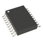 AD7801BRU
The activity of extra discounts on wholesale prices is in full swing…
Please fill in your contact information and we will send you the latest wholesale price list.






