 ChipApex | Global Electronic Components Supplier
AD7863ARZ-10
Search Product
Search Post
— IC芯片 | 连接器 | 传感器 | 被动器件 —
Search productSearch post
— IC芯片 | 连接器 | 传感器 | 被动器件 —
Consult the customer manager about the wholesale price.
consultation hotline:86-132-6715-2157
email:[email protected]
Contact the product manager for consultation. One-stop consultation is available.
Do you want a lower wholesale price? Please send us your inquiry and we will reply immediately.
The AD7863ARZ-10 is a dual 14-bit analog-to-digital converter (ADC) from Analog Devices, operating on a single 5 V supply. It features two simultaneous sampling channels with four total input lines, supporting an analog input range of ±10 V. The device utilizes successive approximation architecture with a conversion time of 5.2 μs and a throughput rate up to 175 kSPS. Key specifications include a typical signal-to-noise ratio of 78 dB, differential nonlinearity of +2/-1 LSB, and integral nonlinearity of ±2.5 LSB. Power consumption is 70 mW in normal mode, dropping to 105 μW maximum in power-down mode.
Verify the specific suffix '10' confirms the ±10 V input voltage range capability. Confirm package type matches system requirements, as the component is available in SOIC_W and SSOP formats. Ensure ordering documentation aligns with the manufacturer's current revision standards to guarantee functional compatibility.
Select this component when simultaneous multi-channel sampling is required without external synchronization hardware. Consider the ±10 V input range specifically for industrial sensor interfaces. Evaluate the 175 kSPS throughput against system bandwidth needs and verify that the parallel interface timing meets the host processor's constraints.
The AD7863 serves as a 14-bit upgrade path for the AD7862 family while maintaining pin compatibility. It integrates two complete ADC functions into a single 28-lead package. The device is fabricated using LC2MOS technology, combining precision bipolar circuits with low-power CMOS logic for optimized performance.
The AD7862 is a related 12-bit predecessor. Verify if the increased resolution and simultaneous sampling capabilities of the AD7863 are necessary for the application before substitution.
The A0 multiplexer select input determines which pair of channels is converted. If A0 is low during conversion initiation, Channel A (VA1/VA2) is selected; if high, Channel B (VB1/VB2) is selected.
The BUSY output goes high upon the falling edge of CONVST and remains high until the conversion process is complete, indicating when data is ready to be read.
Yes, the internal 2.5 V reference is accessible via the VREF pin, but it should be buffered externally due to a nominal source impedance of 5.5 kΩ caused by an internal FET switch.
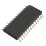 AD7863ARZ-10
The activity of extra discounts on wholesale prices is in full swing…
Please fill in your contact information and we will send you the latest wholesale price list.





