 ChipApex | Global Electronic Components Supplier
AD7878KP
Search Product
Search Post
— IC芯片 | 连接器 | 传感器 | 被动器件 —
Search productSearch post
— IC芯片 | 连接器 | 传感器 | 被动器件 —
Consult the customer manager about the wholesale price.
consultation hotline:86-132-6715-2157
email:[email protected]
Contact the product manager for consultation. One-stop consultation is available.
Do you want a lower wholesale price? Please send us your inquiry and we will reply immediately.
The AD7878KP is a complete 12-bit, 100 kHz sampling Analog-to-Digital Converter (ADC) featuring an integrated DSP interface. It incorporates an on-chip track/hold amplifier with a 2 μs acquisition time, a 3 V zener reference, and an 8-word first-in, first-out (FIFO) memory buffer. The device operates with a bipolar analog input range of ±3 V and utilizes three separate power supplies: +5 V for analog circuits (VDD), +5 V for digital logic (VCC), and -5 V for negative supply (VSS). Key performance metrics include a typical signal-to-noise ratio (SNR) of 72 dB at a 10 kHz input frequency and a maximum data access time of 57 ns. The component is housed in a 28-pin Plastic Leaded Chip Carrier (PLCC) package.
Verify the specific suffix 'KP' corresponds to the 28-pin PLCC package option when sourcing. Confirm that the operating temperature range aligns with the K-grade specification of 0°C to +70°C. Ensure that the design accommodates the required triple power supply rails (+5V, +5V, -5V) and strictly adheres to ESD handling precautions due to the LC2MOS process sensitivity.
Select the AD7878KP when a monolithic solution combining a 12-bit ADC with a dedicated FIFO buffer is required for DSP applications. This model is suitable for designs needing a 72 dB SNR and a 57 ns data access time within commercial temperature limits. Consider alternative packages like the N-28 or Q-28 if different form factors are necessary, while maintaining the same electrical characteristics.
The AD7878 belongs to Analog Devices' family of complete ADCs designed specifically for digital signal processing architectures. Unlike standard converters, this part integrates the necessary interface logic and buffering to minimize processor interrupt latency. The KP variant represents the plastic leaded chip carrier version of the K-grade device, offering a balance between performance and cost for industrial and commercial embedded systems.
Direct pin-compatible replacements within the same package style include the AD7878KN (Plastic DIP) and AD7878LP (Plastic Leaded Chip Carrier). Note that the AD7878LN offers a faster 41 ns access time but requires verification of timing constraints. Military versions such as the AD7878KQ are available via /883B processing if hermetic packaging is required.
The device uses an internal comparator strobe gating mechanism. If a read or write operation occurs during a bit decision, the decision is deferred by one clock cycle to prevent spurious transients from affecting the conversion accuracy.
The BUSY output goes low when the ADC receives a CONVST pulse and remains low until the track/hold enters hold mode. It can be used to disable three-state drivers during this period to prevent bus activity interference.
Yes, provided the DISO bit (DB5) in the status/control register is set to logic 1. If DISO is 0, the data bus outputs are disabled while BUSY is low to prevent transients during the track-to-hold transition.
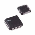 AD7878KP
The activity of extra discounts on wholesale prices is in full swing…
Please fill in your contact information and we will send you the latest wholesale price list.




