 ChipApex | Global Electronic Components Supplier
AD7878SQ
Search Product
Search Post
— IC芯片 | 连接器 | 传感器 | 被动器件 —
Search productSearch post
— IC芯片 | 连接器 | 传感器 | 被动器件 —
Consult the customer manager about the wholesale price.
consultation hotline:86-132-6715-2157
email:[email protected]
Contact the product manager for consultation. One-stop consultation is available.
Do you want a lower wholesale price? Please send us your inquiry and we will reply immediately.
The AD7878SQ is a complete 12-bit analog-to-digital converter featuring an integrated DSP interface with an 8-word FIFO memory. It operates from ±5 V supplies and supports a sampling rate of 100 kSPS. The device includes an on-chip track/hold amplifier, a 3 V zener reference, and status/control logic. Key electrical parameters include a signal-to-noise ratio of 70 dB at 10 kHz input frequency, a maximum data access time of 57 ns, and a typical power dissipation of 60 mW. The analog input range is bipolar ±3 V.
Verify the specific grade suffix SQ corresponds to the -55°C to +125°C operating temperature range and Q-28 package option as listed in the ordering guide. Confirm that the required performance specifications, such as the 70 dB SNR minimum, align with the S version parameters defined in the datasheet tables. Ensure compatibility with the ±5 V supply requirements before integration.
Select the AD7878SQ when an industrial or military temperature range of -55°C to +125°C is required. This model offers a 70 dB SNR and 57 ns data access time, suitable for systems interfacing with processors like the ADSP-2100 or TMS320 series. Consider alternative grades if lower power consumption or higher dynamic performance metrics are prioritized over the extended temperature capability.
The AD7878 is part of Analog Devices' LC2MOS family of complete ADCs designed for high-speed digital signal processing applications. The SQ variant specifically denotes the hermetic ceramic dual-in-line package (Q-28) qualified for the full military temperature range. It shares architectural similarities with other AD78xx series devices but is distinguished by its integrated FIFO and DSP-compatible timing interfaces.
Publicly confirmed substitute part numbers include AD7878JN, AD7878AQ, AD7878KN, AD7878BQ, AD7878LN, AD7878SE4, AD7878JP, AD7878KP, and AD7878LP. Verify that any replacement matches the required temperature range and package style, as these vary across the different suffixes in the ordering guide.
The ADD0 pin determines whether a read operation accesses the data word from Location 0 of the FIFO memory (logic low) or the contents of the status/control register (logic high).
Writing a logic 0 to DB5 (DISO) of the status/control register prevents the data bus from becoming active while the BUSY signal is low, avoiding transients that could affect the track/hold amplifier during acquisition.
The conversion time can slip by up to 17 clock cycles if read or write operations occur during the tLOW periods of the CLK IN signal, potentially extending the total conversion time from 7 µs to 9.12 µs at an 8 MHz clock.
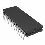 AD7878SQ
The activity of extra discounts on wholesale prices is in full swing…
Please fill in your contact information and we will send you the latest wholesale price list.




