 ChipApex | Global Electronic Components Supplier
AD7892ANZ-1
Search Product
Search Post
— IC芯片 | 连接器 | 传感器 | 被动器件 —
Search productSearch post
— IC芯片 | 连接器 | 传感器 | 被动器件 —
Consult the customer manager about the wholesale price.
consultation hotline:86-132-6715-2157
email:[email protected]
Contact the product manager for consultation. One-stop consultation is available.
Do you want a lower wholesale price? Please send us your inquiry and we will reply immediately.
The AD7892ANZ-1 is a 12-bit successive approximation analog-to-digital converter (ADC) fabricated in Analog Devices' LC2MOS process. It operates from a single +5 V supply and achieves a throughput rate of 500 kSPS with a conversion time of 1.6 µs. The device features an on-chip track/hold amplifier, an internal +2.5 V reference, and signal scaling for ±5 V or ±10 V input ranges. It supports both parallel and serial interfaces via a MODE pin. The component is housed in a 24-lead plastic DIP package and functions within a temperature range of -40 °C to +85 °C.
Verify the specific suffix 'ANZ-1' against the manufacturer's current ordering guide to confirm package type and accuracy grade. Ensure the application requires the specified ±5 V or ±10 V input range compatible with this version. Confirm that the 24-lead PDIP package aligns with the PCB footprint design before finalizing procurement.
Select this model when a 500 kSPS sampling rate and 12-bit resolution are sufficient for the application. It is suitable for designs requiring bipolar input ranges of ±5 V or ±10 V without external scaling circuitry. Consider alternative versions if higher throughput rates or different input voltage ranges are required.
The AD7892 belongs to a family of high-speed, low-power ADCs designed for single-supply operation. Variants within the series differ primarily in input voltage ranges and maximum throughput speeds. This specific part represents the standard accuracy version optimized for general-purpose applications.
Direct replacements include other AD7892 variants such as AD7892BN-1 for improved accuracy or AD7892AR-1 for surface mount packaging. Verify pin compatibility and electrical specifications before substituting.
The input range is determined by the connection of the VIN2 pin. Connecting VIN2 to AGND sets the range to ±10 V, while connecting VIN2 to VIN1 sets it to ±5 V.
The MODE pin selects the data output interface. A logic high selects the parallel interface mode, while a logic low selects the serial interface mode.
Yes, the internal +2.5 V reference is available at the REF OUT/REF IN pin. However, it should be buffered externally if driving loads beyond the chip's internal buffer capability due to its nominal 5.5 kΩ output impedance.
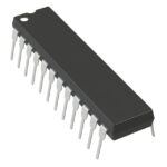 AD7892ANZ-1
The activity of extra discounts on wholesale prices is in full swing…
Please fill in your contact information and we will send you the latest wholesale price list.




