 ChipApex | Global Electronic Components Supplier
AD7892AR-1
Search Product
Search Post
— IC芯片 | 连接器 | 传感器 | 被动器件 —
Search productSearch post
— IC芯片 | 连接器 | 传感器 | 被动器件 —
Consult the customer manager about the wholesale price.
consultation hotline:86-132-6715-2157
email:[email protected]
Contact the product manager for consultation. One-stop consultation is available.
Do you want a lower wholesale price? Please send us your inquiry and we will reply immediately.
The AD7892AR-1 is a high-speed, low-power 12-bit analog-to-digital converter (ADC) fabricated in Analog Devices' LC2MOS process. It operates from a single +5 V supply and features an on-chip track/hold amplifier and internal +2.5 V reference. The device supports ±10 V or ±5 V analog input ranges with overvoltage protection up to ±17 V. It offers a throughput rate of 500 kSPS with a conversion time of 1.6 µs. The part provides flexible parallel and serial interface options for microprocessor connectivity and is housed in a 24-lead SOIC package.
Verify the specific suffix 'AR-1' to confirm the ±10 V/±5 V input range and 500 kSPS throughput specification. Ensure the ordering matches the required temperature grade and package type. Cross-reference the manufacturer's latest datasheet revision to confirm pinout compatibility and absolute maximum ratings before integration into new designs.
Select this model when bipolar input signals within ±10 V are required alongside low power consumption. Compare against AD7892-3 if higher 600 kSPS throughput is needed with a smaller ±2.5 V input range. Consider the AD7892-2 for unipolar 0 V to +2.5 V applications. Verify that the system clocking can accommodate the 1.6 µs conversion time for the specified sample rate.
This component belongs to the AD7892 family of single-supply ADCs. It shares the core LC2MOS architecture and interface logic with variants offering different input ranges and throughput rates. The 'AR' designation indicates the SOIC package, while '-1' specifies the bipolar input configuration. It serves as a bridge between high-speed conversion and low-power portable design constraints.
AD7892BR-1: Offers improved relative accuracy (±1 LSB) compared to the AR version. AD7892AN-1: Plastic DIP package alternative with identical electrical specifications. AD7892BN-1: Improved accuracy in plastic DIP format. Ensure pinout compatibility remains consistent across these package and accuracy variations.
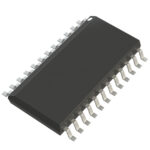 AD7892AR-1
The activity of extra discounts on wholesale prices is in full swing…
Please fill in your contact information and we will send you the latest wholesale price list.




