 ChipApex | Global Electronic Components Supplier
AD7893AN-5
Search Product
Search Post
— IC芯片 | 连接器 | 传感器 | 被动器件 —
Search productSearch post
— IC芯片 | 连接器 | 传感器 | 被动器件 —
Consult the customer manager about the wholesale price.
consultation hotline:86-132-6715-2157
email:[email protected]
Contact the product manager for consultation. One-stop consultation is available.
Do you want a lower wholesale price? Please send us your inquiry and we will reply immediately.
The AD7893AN-5 is a 12-bit successive approximation analog-to-digital converter (ADC) housed in an 8-pin plastic DIP package. It operates from a single +5 V supply and features an on-chip track/hold amplifier, internal clock, and high-speed serial interface. The device accepts an analog input range of 0 V to +5 V with a typical power dissipation of 25 mW. Key electrical specifications include a maximum conversion time of 6 μs, a throughput rate up to 117 kHz, and a signal-to-noise ratio of 70 dB. Relative accuracy is specified at ±1 LSB, with differential nonlinearity and integral nonlinearity both within ±1 LSB.
Verify the specific ordering suffix AN-5 corresponds to the required 8-pin plastic DIP package and the 0 V to +5 V input voltage range. Confirm that the -40 °C to +85 °C commercial temperature rating aligns with the operational environment requirements before finalizing procurement.
Select this component when a compact 8-pin solution is required for 12-bit resolution with a unipolar 0 V to +5 V input range. Ensure the system design accommodates the external +2.5 V reference voltage requirement and the specific timing constraints associated with the serial read operation during or after conversion.
This part belongs to the AD7893 family of fast 12-bit ADCs fabricated using Linear Compatible CMOS (LC2MOS) technology. The family includes variants with different input ranges such as ±10 V, ±2.5 V, and 0 V to +2.5 V, as well as options for SOIC and Cerdip packages. The AD7893AN-5 specifically denotes the plastic DIP version optimized for the 0 V to +5 V unipolar application.
Direct pin-compatible replacements within the same series include AD7893BN-5 for improved linearity or AD7893AR-5 for surface mount integration. Cross-family migration may require schematic adjustments due to differences in reference requirements or interface protocols.
The AD7893AN-5 uses straight (natural) binary output coding.
Conversion is initiated by the rising edge of the CONVST input signal, which triggers the track/hold amplifier to enter hold mode.
To achieve optimum performance, a minimum of 600 ns should be allowed after the read operation ends and before the next rising edge of CONVST.
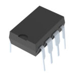 AD7893AN-5
The activity of extra discounts on wholesale prices is in full swing…
Please fill in your contact information and we will send you the latest wholesale price list.





