 ChipApex | Global Electronic Components Supplier
AD7899ARZ-3
Search Product
Search Post
— IC芯片 | 连接器 | 传感器 | 被动器件 —
Search productSearch post
— IC芯片 | 连接器 | 传感器 | 被动器件 —
Consult the customer manager about the wholesale price.
consultation hotline:86-132-6715-2157
email:[email protected]
Contact the product manager for consultation. One-stop consultation is available.
Do you want a lower wholesale price? Please send us your inquiry and we will reply immediately.
The AD7899ARZ-3 is a 14-bit successive-approximation analog-to-digital converter (ADC) operating from a single 5 V supply. It delivers a maximum throughput rate of 400 kSPS with a conversion time of 2.2 µs and a track/hold acquisition time of 0.3 µs. The device features an internal 2.5 V reference, on-chip clock oscillator, and signal conditioning circuitry. It accepts bipolar input ranges of ±2.5 V and utilizes a high-speed parallel interface compatible with 3 V or 5 V processors. Typical power consumption is 80 mW in normal mode, reducing to 20 µW in standby.
Verify the specific suffix '-3' corresponds to the ±2.5 V input range variant before integration. Confirm that the SOIC-28 package thermal characteristics meet the system's dissipation requirements. Ensure the design accounts for the 0.1 µF decoupling capacitor required on the VREF pin to maintain reference stability during operation.
Select this component when a single-channel, 14-bit resolution is required with a ±2.5 V input span. The AD7899ARZ-3 is suitable for applications needing fast conversion speeds up to 400 kSPS while maintaining low power consumption. Consider the parallel interface complexity versus serial alternatives if board space or pin count is constrained.
The AD7899 series includes variants with different input ranges: AD7899-1 for ±10 V/±5 V, AD7899-2 for 0 V to 5 V/2.5 V, and AD7899-3 for ±2.5 V. All share the same 14-bit SAR architecture and 400 kSPS throughput capability. The ARZ designation indicates a lead-free, RoHS-compliant SOIC-28 package version within the Analog Devices portfolio.
Public confirmed substitute part numbers are not available in the provided documentation.
The clock source is determined by the state of the CLKIN pin at the rising edge of CONVST. If CLKIN is high, an external clock is used; if low, the internal oscillator is engaged.
The BUSY/EOC pin signals the status of the conversion. It goes high when CONVST rises and remains high until the conversion completes, indicating either busy status or end-of-conversion depending on the CONVST state.
Yes, the VREF pin provides access to the internal 2.5 V reference. However, it has a nominal output impedance of 6 kΩ, so buffering is recommended if driving external loads.
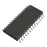 AD7899ARZ-3
The activity of extra discounts on wholesale prices is in full swing…
Please fill in your contact information and we will send you the latest wholesale price list.





