 ChipApex | Global Electronic Components Supplier
AD7899SR-1
Search Product
Search Post
— IC芯片 | 连接器 | 传感器 | 被动器件 —
Search productSearch post
— IC芯片 | 连接器 | 传感器 | 被动器件 —
Consult the customer manager about the wholesale price.
consultation hotline:86-132-6715-2157
email:[email protected]
Contact the product manager for consultation. One-stop consultation is available.
Do you want a lower wholesale price? Please send us your inquiry and we will reply immediately.
The AD7899SR-1 is a 14-bit successive-approximation analog-to-digital converter (ADC) from Analog Devices, designed for high-speed data acquisition. It operates on a single 5 V supply with typical power consumption of 80 mW and features a maximum throughput rate of 400 kSPS. The device includes an internal 2.5 V reference, track/hold amplifier, and on-chip clock oscillator. It supports input ranges of ±5 V and ±10 V with overvoltage protection up to ±18 V. The part utilizes a high-speed parallel interface compatible with 3 V or 5 V logic levels and is housed in a 28-lead SOIC package.
Verify the specific suffix 'SR-1' corresponds to the military temperature grade (-55°C to +125°C) and ±10 V/±5 V input range configuration. Confirm package type is Small Outline (SOIC). Ensure compatibility with system voltage requirements for VDD and VDRIVE pins before integration.
Select this component when a 14-bit resolution and 400 kSPS throughput are required within a single-supply architecture. The AD7899SR-1 is suitable for environments demanding extended temperature stability. Consider the parallel interface complexity versus serial alternatives if pin count is constrained.
The AD7899 series comprises three versions differentiated by input range: -1 for bipolar ±5 V/±10 V, -2 for unipolar 0 V to 2.5 V/5 V, and -3 for ±2.5 V. The 'S' suffix denotes the military-grade temperature range variant, while 'A' and 'B' denote commercial grades with varying accuracy specifications.
Publicly confirmed substitute part numbers are not available in the provided documentation. Designers should evaluate other SAR ADCs with similar throughput and resolution if sourcing constraints exist.
The AD7899SR-1 uses an internally laser-trimmed clock oscillator by default. An external clock can be applied to the CLKIN pin; if CLKIN is high on the rising edge of CONVST, the external clock is used.
The STBY pin controls the standby mode. Driving this pin low places the device into a power-saving state with typical current consumption of 20 µA, while keeping it high enables normal operation.
Yes. The VREF pin provides access to the internal 2.5 V reference but also allows an external precision 2.5 V reference to be connected, which will effectively overdrive the internal source.
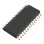 AD7899SR-1
The activity of extra discounts on wholesale prices is in full swing…
Please fill in your contact information and we will send you the latest wholesale price list.




