 ChipApex | Global Electronic Components Supplier
AD7960BCPZ
Search Product
Search Post
— IC芯片 | 连接器 | 传感器 | 被动器件 —
Search productSearch post
— IC芯片 | 连接器 | 传感器 | 被动器件 —
Consult the customer manager about the wholesale price.
consultation hotline:86-132-6715-2157
email:[email protected]
Contact the product manager for consultation. One-stop consultation is available.
Do you want a lower wholesale price? Please send us your inquiry and we will reply immediately.
The AD7960BCPZ is an 18-bit, 5 MSPS PulSAR differential analog-to-digital converter (ADC) manufactured by Analog Devices Inc. It features a charge redistribution successive approximation register (SAR) architecture with no pipeline latency. The device supports true differential analog inputs ranging from ±4.096 V to ±5 V and operates on dual supplies of 5 V and 1.8 V. Key performance metrics include a signal-to-noise ratio (SNR) of 99 dB, total harmonic distortion (THD) of −117 dB, integral nonlinearity (INL) of ±0.8 LSB typical, and differential nonlinearity (DNL) of ±0.5 LSB typical. Power consumption is 39 mW in self-clocked mode with an external reference buffer. It utilizes a serial LVDS interface for data output and is housed in a 32-lead LFCSP package.
Verify the specific ordering suffix against the manufacturer's current datasheet to confirm package type and temperature range specifications. Ensure compatibility with required supply voltages and reference configurations before finalizing procurement orders.
Select this component for applications requiring high linearity and low noise at moderate sampling rates. Consider the internal reference buffer if board space is limited; otherwise, use an external reference for potentially lower power consumption. Verify that the host system supports LVDS signaling for the data interface.
The AD7960 belongs to the PulSAR family of ADCs from Analog Devices, designed for precision data acquisition. It complements other models like the AD7961 and AD7982 within the same series, offering a balance between resolution, speed, and power efficiency suitable for industrial and medical instrumentation.
Direct substitutes within the same family include the AD7960BCPZ-RL7, which shares identical electrical characteristics but differs in packaging format as a reel product rather than cut tape.
The -3 dB input bandwidth is 28 MHz when EN2 is set to 0. Setting EN2 to 1 reduces the bandwidth to 9 MHz for throughput rates of 2 MSPS or lower.
The CNV+ and CNV- pins can accept either CMOS or LVDS format signals. When CNV- is grounded, CNV+ functions as a single-ended CMOS input.
The device supports an internal reference buffer driven by a 2.048 V external reference, or direct external references of 4.096 V or 5 V applied to the REF pin.
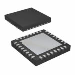 AD7960BCPZ
The activity of extra discounts on wholesale prices is in full swing…
Please fill in your contact information and we will send you the latest wholesale price list.




