 ChipApex | Global Electronic Components Supplier
SEARCH
Search Product
Search Post
— IC芯片 | 连接器 | 传感器 | 被动器件 —
Search productSearch post
— IC芯片 | 连接器 | 传感器 | 被动器件 —
Consult the customer manager about the wholesale price.
consultation hotline:86-132-6715-2157
email:[email protected]
Contact the product manager for consultation. One-stop consultation is available.
Do you want a lower wholesale price? Please send us your inquiry and we will reply immediately.
The AD8185ARUZ is a high-speed triple 2:1 multiplexer manufactured by Analog Devices Inc., housed in a 24-lead TSSOP package. It operates on ±5 V supplies with a quiescent current of 25 mA. The device provides a voltage gain of +2, achieving a –3 dB bandwidth of up to 360 MHz for small signals and 300 MHz for large signals at 2 V p-p. Key performance metrics include a slew rate of 1150 V/µs, a settling time of 15 ns to 0.1%, and an OFF isolation of –100 dB at 10 MHz. It supports an operating temperature range from –40°C to +85°C.
Verify the specific ordering suffix against the manufacturer's official documentation to ensure correct packaging options. Confirm that the component meets RoHS compliance requirements for your target market. Cross-reference the part number with authorized distributors to validate authenticity and supply chain integrity before finalizing procurement decisions.
Select the AD8185ARUZ when a non-inverting gain of +2 is required for RGB video signals. Ensure the design accommodates ±5 V power supplies and considers the thermal dissipation characteristics of the 24-lead TSSOP package. Verify that the load impedance matches the specified conditions for optimal bandwidth and crosstalk performance.
This component belongs to the AD8183/AD8185 family of high-speed triple 2:1 multiplexers. While the AD8183 offers unity gain, the AD8185 variant provides a gain of +2, making it suitable for driving reverse-terminated video loads without external amplification. Both devices share similar switching speeds and power consumption profiles within the same package.
The AD8183ARUZ serves as a functional substitute if a gain of +1 is acceptable for the application. Other variants within the AD8183/AD8185 series may be considered based on specific packaging or reel requirements, provided the electrical parameters align with the system design.
To minimize peaking and ensure stability when driving large capacitive loads, a small series resistor should be added between the output and the load capacitor.
The OE (Output Enable) pin controls whether the three outputs are enabled or disabled into a high-impedance state, allowing for bus sharing and reduced power consumption.
The device offers high OFF isolation of –100 dB at 10 MHz, ensuring minimal signal leakage from disconnected channels.
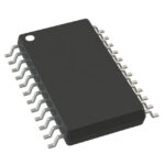 AD8185ARUZ
The activity of extra discounts on wholesale prices is in full swing…
Please fill in your contact information and we will send you the latest wholesale price list.





