 ChipApex | Global Electronic Components Supplier
SEARCH
Search Product
Search Post
— IC芯片 | 连接器 | 传感器 | 被动器件 —
Search productSearch post
— IC芯片 | 连接器 | 传感器 | 被动器件 —
Consult the customer manager about the wholesale price.
consultation hotline:86-132-6715-2157
email:[email protected]
Contact the product manager for consultation. One-stop consultation is available.
Do you want a lower wholesale price? Please send us your inquiry and we will reply immediately.
The AD829AQ is a high-speed, low-noise video operational amplifier manufactured by Analog Devices Inc. It features a gain bandwidth product of 600 MHz at ±5 V and 750 MHz at ±15 V, with an uncompensated slew rate of 230 V/µs. The device maintains a bandwidth greater than 50 MHz for gains ranging from 1 to 20 through external compensation. Key performance metrics include a maximum input offset voltage of 0.5 mV over the temperature range, 1.7 nV/√Hz input voltage noise, and 1.5 pA/√Hz input current noise. It offers excellent differential gain (0.02%) and phase error (0.04°) at standard video frequencies.
Verify that the ordering suffix AQ corresponds to the extended temperature range specification (-40°C to +125°C) and the tighter input offset voltage maximum of 0.5 mV as defined in the manufacturer's specifications table. Confirm package availability matches the required form factor, such as CERDIP or SOIC, ensuring compatibility with the intended PCB layout and thermal management requirements.
Select this component when application requirements demand a balance between high speed and low noise. The external compensation feature provides flexibility to tailor bandwidth and slew rate trade-offs based on the closed-loop gain. Ensure the supply voltage range aligns with the ±5 V to ±15 V operating limits and verify that the load impedance does not exceed the specified output swing capabilities.
The AD829 series comprises high-speed video operational amplifiers designed for demanding signal processing tasks. The AD829AQ variant specifically targets industrial and military environments requiring operation across an extended temperature range. It belongs to a family of devices characterized by complementary bipolar fabrication processes that support high transconductance and low noise performance.
The AD829S is a qualified military-grade alternative within the same family offering similar electrical characteristics but potentially different reliability standards. Verify pinout compatibility and thermal resistance differences if substituting between package types such as CERDIP and SOIC.
The external compensation pin allows users to adjust the frequency response by adding capacitance. This enables customization of the bandwidth and slew rate trade-off for specific closed-loop gains, optimizing the device for either high-speed settling or wider bandwidth.
For the AD829AQ variant, the maximum input offset voltage is specified as 0.5 mV over the full temperature range, which is tighter than the 1 mV maximum found in other variants like the AD829JR.
Yes, the AD829 is designed to drive heavy capacitive loads. Internal circuitry, including bootstrapping techniques, helps maintain stability and phase margin even when significant capacitance is present at the output.
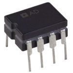 AD829AQ
The activity of extra discounts on wholesale prices is in full swing…
Please fill in your contact information and we will send you the latest wholesale price list.





