 ChipApex | Global Electronic Components Supplier
SEARCH
Search Product
Search Post
— IC芯片 | 连接器 | 传感器 | 被动器件 —
Search productSearch post
— IC芯片 | 连接器 | 传感器 | 被动器件 —
Consult the customer manager about the wholesale price.
consultation hotline:86-132-6715-2157
email:[email protected]
Contact the product manager for consultation. One-stop consultation is available.
Do you want a lower wholesale price? Please send us your inquiry and we will reply immediately.
The AD829AR is a high-speed, low-noise video operational amplifier manufactured by Analog Devices Inc. It features a gain bandwidth product of 750 MHz at ±15 V and a slew rate of 230 V/µs. The device maintains a bandwidth greater than 50 MHz for gains ranging from 1 to 20 through external compensation. Key performance metrics include an input voltage noise of 1.7 nV/√Hz, a maximum input offset voltage of 1 mV over the temperature range, and differential gain/phase errors of 0.02% and 0.04° respectively at standard video frequencies. It operates on supply voltages between ±5 V and ±15 V with a quiescent current of approximately 5 mA.
Verify the suffix 'AR' corresponds to the industrial temperature range (-40°C to +125°C) and SOIC package as specified in the ordering guide. Confirm that the component matches the Rev. I datasheet specifications regarding offset voltage and bandwidth. Ensure compatibility with existing board layouts for the 8-lead SOIC footprint before finalizing procurement.
Select the AD829AR when application requirements demand high slew rates combined with low noise in a voltage feedback architecture. It is preferred over transimpedance amplifiers where lower current noise is critical. Consider this part for designs needing flexible gain settings up to 20 while maintaining consistent bandwidth, or for systems requiring output clamping capabilities via the compensation pin.
The AD829 series includes variants such as the AD829J for commercial temperatures and the AD829S for military specifications. The AD829AR specifically denotes the industrial grade version housed in an 8-lead Small Outline Integrated Circuit (SOIC) package. This family is designed for applications requiring fast settling times and high dynamic range in professional video and data acquisition environments.
Public confirmed substitute part numbers are not provided in the source material.
The external compensation pin allows users to customize the frequency response. By adjusting the compensation capacitance, the bandwidth can be optimized for a given load and supply voltage, or the output can be clamped.
The maximum input offset voltage for the AD829AR is 1 mV over the full operating temperature range of -40°C to +125°C.
Yes, the AD829 is capable of driving heavy capacitive loads due to its internal circuit design which buffers the compensation node from the output stage.
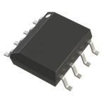 AD829AR
The activity of extra discounts on wholesale prices is in full swing…
Please fill in your contact information and we will send you the latest wholesale price list.





