 ChipApex | Global Electronic Components Supplier
SEARCH
Search Product
Search Post
— IC芯片 | 连接器 | 传感器 | 被动器件 —
Search productSearch post
— IC芯片 | 连接器 | 传感器 | 被动器件 —
Consult the customer manager about the wholesale price.
consultation hotline:86-132-6715-2157
email:[email protected]
Contact the product manager for consultation. One-stop consultation is available.
Do you want a lower wholesale price? Please send us your inquiry and we will reply immediately.
The AD8310ARMZ-REEL7 is a demodulating logarithmic amplifier from Analog Devices Inc. It operates from DC to 440 MHz with a 95 dB dynamic range, defined from −91 dBV to +4 dBV. The device features a voltage output with a slope of +24 mV/dB and an intercept of −108 dBV. It utilizes a single supply voltage ranging from 2.7 V to 5.5 V, drawing a typical quiescent current of 8 mA. The component provides a fast rise time of less than 15 ns and can drive up to 25 mA into a grounded load. It is housed in an 8-lead MSOP package.
Verify the specific ordering suffix REEL7 confirms tape and reel packaging when sourcing. Confirm the manufacturer is Analog Devices Inc. and the part status is active. Ensure the operating temperature range meets industrial requirements of -40°C to +85°C. Cross-reference the datasheet revision F specifications against the received component lot.
Select this component for applications requiring accurate logarithmic conversion from audio frequencies up to UHF ranges. The fully differential input simplifies matching to source impedances. Consider the 24 mV/dB slope for output scaling compatibility with downstream ADCs or controllers. Verify that the 95 dB dynamic range covers the expected signal amplitude variations in the target system.
This component belongs to the AD8310 series of logarithmic amplifiers manufactured by Analog Devices Inc. It is designed as a complete solution for RF and baseband signal detection. The device integrates six amplifier stages and nine detector cells on a single die. It represents a specialized class of analog signal processing ICs used for precise envelope detection and level monitoring.
Consult official documentation for direct pin-compatible substitutes within the same family. Verify functional equivalence regarding dynamic range and bandwidth if considering alternative manufacturers.
The device supports operation down to very low frequencies, including audio ranges, by utilizing an external capacitor at the OFLT pin to lower the high-pass corner frequency of the offset compensation loop.
The ENBL pin serves as a CMOS-compatible chip enable. Applying a high voltage activates the device, while a low voltage disables it, reducing the supply current to a sleep mode of approximately 1 mA.
Yes, the standard slope of 24 mV/dB can be altered using external resistors connected to the BFIN pin, allowing customization of the transfer function for specific application needs.
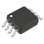 AD8310ARMZ-REEL7
The activity of extra discounts on wholesale prices is in full swing…
Please fill in your contact information and we will send you the latest wholesale price list.





