 ChipApex | Global Electronic Components Supplier
SEARCH
Search Product
Search Post
— IC芯片 | 连接器 | 传感器 | 被动器件 —
Search productSearch post
— IC芯片 | 连接器 | 传感器 | 被动器件 —
Consult the customer manager about the wholesale price.
consultation hotline:86-132-6715-2157
email:[email protected]
Contact the product manager for consultation. One-stop consultation is available.
Do you want a lower wholesale price? Please send us your inquiry and we will reply immediately.
The AD8328 is a 5 V upstream cable line driver designed for DOCSIS and EuroDOCSIS reverse path transmission. It features digitally programmable gain in 1 dB steps over a 59 dB range, controlled via an SPI interface. The device maintains a 300 Ω differential output impedance, suitable for driving 75 Ω loads through a 2:1 transformer. Key performance metrics include -57.5 dBc SFDR at 21 MHz and -54 dBc at 65 MHz with a 60 dBmV output. Output noise is 1.2 nV/√Hz at minimum gain, with an upper bandwidth of 107 MHz across the full gain range.
Verify component authenticity through authorized Analog Devices distributors or direct manufacturer channels. Confirm package type (LFCSP or QSOP) and temperature grade (-40°C to +85°C) matches design requirements. Check for obsolete status indicators as the datasheet marks this part as obsolete; ensure availability of long-term supply agreements or alternative sourcing strategies if required for production continuity.
Select the AD8328 for applications requiring precise digital gain control in upstream cable paths. Ensure the system supports a single 5 V supply and provides necessary SPI control lines. Verify that the input signal can be AC-coupled to the VCC/2 bias point. Consider thermal management for LFCSP packages on standard PCBs, noting the specific thermal resistance values provided in the absolute maximum ratings section.
The AD8328 serves as a low-cost amplifier specifically engineered for coaxial line driving in cable modem architectures. It integrates an input amplifier, vernier control, and output stage to handle QPSK and QAM signals. The device replaces discrete solutions by providing integrated gain programming, distortion optimization, and power management features within a compact 20-lead package format.
Public documentation indicates the AD8328 is marked as obsolete. Designers should evaluate the AD8324 as a potential functional substitute for similar upstream cable driver applications, noting differences in supply voltage (3.3 V vs. 5 V) and packaging options. Verify pin compatibility and electrical specifications against the new component's datasheet before implementation.
The AD8328 maintains a 300 Ω differential output impedance regardless of whether the TXEN pin is high or low, ensuring proper matching to 75 Ω loads via a 2:1 transformer without external back termination resistors.
The RAMP pin controls the duration of burst on/off transients. Leaving it unconnected ensures compliance with DOCSIS 2.0 spurious emission requirements by dissipating transients no faster than 2 μs.
Yes, the AD8328 accepts either differential or single-ended input signals. For single-ended operation, the input impedance is approximately 800 Ω, while differential input impedance is 1.6 kΩ.
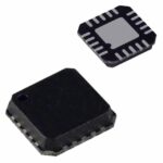 AD8328ACPZ-REEL
The activity of extra discounts on wholesale prices is in full swing…
Please fill in your contact information and we will send you the latest wholesale price list.







