 ChipApex | Global Electronic Components Supplier
SEARCH
Search Product
Search Post
— IC芯片 | 连接器 | 传感器 | 被动器件 —
Search productSearch post
— IC芯片 | 连接器 | 传感器 | 被动器件 —
Consult the customer manager about the wholesale price.
consultation hotline:86-132-6715-2157
email:[email protected]
Contact the product manager for consultation. One-stop consultation is available.
Do you want a lower wholesale price? Please send us your inquiry and we will reply immediately.
The AD8398A is a dual-channel, voltage-feedback operational amplifier designed for high-speed line driver applications. It operates on a single +12 V or dual ±6 V supply. Key electrical parameters include an 85 MHz bandwidth (at AV DIFF = 5), a 600 V/µs slew rate, and a linear peak output current of 450 mA. The device delivers an 18.4 V p-p differential swing into a 20 Ω load. It features four power modes controlled by PD0 and PD1 pins, reducing quiescent current to 0.7 mA in power-down mode.
Verify the specific ordering suffix (R2, R7, or RL) against the required reel quantity, as these denote different packaging formats rather than functional differences. Confirm RoHS compliance status, indicated by the 'Z' suffix in the part number. Ensure the design accounts for the thermally enhanced package requirements, specifically connecting the exposed paddle to a ground plane for optimal thermal dissipation.
Select this component when designing systems requiring high differential output swing and significant drive current into low impedance loads like 20 ohms. The dual-channel architecture allows for cost-effective implementation of balanced line drivers. Consider the available power modes if system standby current consumption is a critical constraint, as the device supports deep power-down states.
The AD8398A belongs to Analog Devices' portfolio of specialized amplifiers tailored for telecommunications infrastructure. It is part of the AD8398 series, which focuses on providing robust solutions for xDSL and PLC applications. The device integrates two independent amplifiers into a single compact package, simplifying board layout compared to discrete solutions while maintaining high performance metrics.
Publicly confirmed substitutes are not identified in the provided documentation. When evaluating alternatives, ensure compatibility with the 16-lead LFCSP_WQ footprint and verify that replacement devices meet the 450 mA peak output current and 85 MHz bandwidth requirements for VDSL2 Profile 8b and 17a applications.
The device incorporates two CMOS-compatible control pins, PD0 and PD1, which select from four operating modes: full power, medium power, low power, and complete power-down. In power-down mode, the quiescent current drops to 0.7 mA.
The exposed paddle is electrically isolated but serves as a thermal pad. It should be connected to a solid ground plane layer with low thermal resistance to ensure adequate heat transfer away from the die and maintain junction temperature below 125°C.
Yes. Because DSL line drivers are transformer-coupled to twisted pairs, they may be subject to large transients from lightning strikes or downed power lines. Additional circuitry is required to protect the AD8398A from damage due to these events.
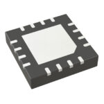 AD8398ACPZ-RL
The activity of extra discounts on wholesale prices is in full swing…
Please fill in your contact information and we will send you the latest wholesale price list.






