 ChipApex | Global Electronic Components Supplier

SEARCH
Search Product
Search Post
— IC芯片 | 连接器 | 传感器 | 被动器件 —
Search productSearch post
— IC芯片 | 连接器 | 传感器 | 被动器件 —
Consult the customer manager about the wholesale price.
consultation hotline:86-132-6715-2157
email:[email protected]
Contact the product manager for consultation. One-stop consultation is available.
Do you want a lower wholesale price? Please send us your inquiry and we will reply immediately.
The AD8402ANZ10 is a dual-channel, 256-position digital potentiometer manufactured by Analog Devices Inc. It operates on a single supply voltage ranging from 2.7 V to 5.5 V and features a nominal resistance of 10 kΩ with a ±1% channel-to-channel matching tolerance. The device utilizes an SPI-compatible 3-wire serial interface for data input and includes volatile memory to retain wiper settings upon power cycling. Key electrical parameters include a typical wiper resistance of 100 Ω at 5 V, a temperature coefficient of 500 ppm/°C, and a shutdown current of less than 5 μA. It is housed in a 14-lead PDIP package.
Verify the specific suffix 'ANZ' against the manufacturer's official ordering guide to confirm the package type (PDIP) and RoHS compliance status. Confirm availability as this component may be subject to obsolescence or lifecycle changes. Ensure the selected variant matches the required pin configuration and thermal characteristics for the target PCB design.
Select the AD8402ANZ10 when a dual-channel solution with 10 kΩ nominal resistance is required. The 'N' suffix indicates a PDIP package suitable for through-hole mounting. Verify that the application supports volatile memory behavior, as wiper positions are lost during power loss unless retained externally. Ensure the serial interface logic levels are compatible with the 2.7 V to 5.5 V supply range.
The AD8402ANZ10 belongs to the AD8400/AD8402/AD8403 family of digital potentiometers. This family provides digitally controlled variable resistors available in single, dual, and quad-channel configurations. The AD8402 specifically offers two independent channels in space-saving packages, allowing for precise electronic adjustment functions similar to mechanical potentiometers.
Direct substitutes within the same family include the AD8402ARZ10 (SOIC-14 package) and AD8402ARUZ10 (TSSOP-14 package). These alternatives share identical electrical specifications but differ in physical footprint and mounting style. Cross-package replacements require PCB layout modifications.
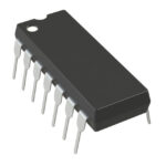 AD8402ANZ10

The activity of extra discounts on wholesale prices is in full swing…
Please fill in your contact information and we will send you the latest wholesale price list.





