 ChipApex | Global Electronic Components Supplier
AD8522JRU
Search Product
Search Post
— IC芯片 | 连接器 | 传感器 | 被动器件 —
Search productSearch post
— IC芯片 | 连接器 | 传感器 | 被动器件 —
Consult the customer manager about the wholesale price.
consultation hotline:86-132-6715-2157
email:[email protected]
Contact the product manager for consultation. One-stop consultation is available.
Do you want a lower wholesale price? Please send us your inquiry and we will reply immediately.
The AD8522JRU is a dual 12-bit digital-to-analog converter (DAC) from Analog Devices Inc., housed in a 14-lead SOIC surface-mount package. It operates on a single +5 V supply and features a serial digital interface with daisy-chain capability via the SDO pin. The device integrates a laser-trimmed 2.5 V bandgap reference and buffered voltage outputs capable of driving ±5 mA loads. Key electrical specifications include a typical settling time of 16 μs to ±1 LSB, a full-scale output of 4.095 V, and an operating temperature range of –40°C to +85°C.
Verify that the ordering suffix 'JRU' corresponds to the specified 14-lead SOIC package and the industrial temperature range of –40°C to +85°C. Confirm compliance with RoHS standards as indicated by the 'Z' suffix in the standard part number AD8522AR. Ensure the source documentation explicitly validates this specific suffix variant against the official Analog Devices ordering guide.
Select the AD8522JRU for applications requiring low power consumption (5 mW/DAC) and minimal external components in space-constrained designs. The device is suitable for microcontroller interfaces due to its simple three-wire serial protocol. Consider the 16 μs settling time and ±1.5 LSB relative accuracy when designing for precision analog signal generation.
The AD8522 series consists of complete dual 12-bit DACs fabricated in a CBCMOS process. While the datasheet lists the AD8522AR for the SOIC-14 package, the AD8522JRU represents a specific commercial or industrial variant within this family. The component eliminates the need for external references or buffers, offering a cost-effective solution for single-supply systems.
The AD8522AR is the documented equivalent for the 14-lead SOIC package. Verify if the 'J' suffix indicates a specific temperature grade or manufacturing lot difference compared to the standard 'A' suffix before substitution.
It supports two modes: hardware-load, where external LDA/LDB pins trigger updates, and software-decode, where the internal logic uses address bits A and B to select the target DAC register.
The output amplifiers are characterized to drive up to 500 pF of capacitive load without oscillation.
Yes, while fully specified for +4.5 V to +5.5 V, operation down to +4.3 V is possible if reduced linearity and source current near full scale are acceptable.
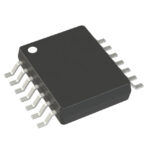 AD8522JRU
The activity of extra discounts on wholesale prices is in full swing…
Please fill in your contact information and we will send you the latest wholesale price list.





