 ChipApex | Global Electronic Components Supplier
AD9129BBC
Search Product
Search Post
— IC芯片 | 连接器 | 传感器 | 被动器件 —
Search productSearch post
— IC芯片 | 连接器 | 传感器 | 被动器件 —
Consult the customer manager about the wholesale price.
consultation hotline:86-132-6715-2157
email:[email protected]
Contact the product manager for consultation. One-stop consultation is available.
Do you want a lower wholesale price? Please send us your inquiry and we will reply immediately.
The AD9129BBCZ is a high-performance, 14-bit RF digital-to-analog converter (DAC) manufactured by Analog Devices Inc. It supports data rates up to 2.85 GSPS in normal mode and achieves an effective update rate of 5.7 GSPS when configured for Mix-Mode or 2× interpolation. The device utilizes a quad-switch architecture to enable dual-edge clocking, facilitating direct RF synthesis in the second and third Nyquist zones up to 4.2 GHz. Key electrical parameters include a full-scale output current range of 9.5 mA to 34.4 mA, integral nonlinearity (INL) of ±1.4 LSB, and differential nonlinearity (DNL) of ±1.1 LSB. It operates from +1.8 V analog/digital supplies and −1.5 V analog supply, consuming approximately 1.0 W at 2.85 GSPS.
Verify the specific ordering suffix against the manufacturer's official documentation to confirm package type, temperature range, and reel/tray packaging details. Ensure compatibility with system voltage requirements (+1.8 V digital/analog, -1.5 V analog) and interface standards (LVDS/DHSTL). Confirm moisture sensitivity level handling during storage and assembly.
Select this component for applications requiring high linearity and wide bandwidth in RF signal generation. Consider the Mix-Mode operation if synthesizing carriers in higher Nyquist zones is required. Evaluate power consumption constraints, as dissipation increases with data rate and filter settings (FIR25/FIR40). Ensure the host FPGA/ASIC can support the dual-port LVDS interface and maximum clock rates.
The AD9129 is part of the AD9119/AD9129 family of RF DACs, differentiated primarily by resolution (14-bit vs. 11-bit). Both share the same quad-switch architecture and interface capabilities. The BBCZ suffix typically denotes a specific commercial grade and BGA-160 package variant within the Analog Devices portfolio.
The AD9119BBCZ is a compatible alternative within the same family, offering identical functionality but with 11-bit resolution instead of 14-bit. Verify that the reduced resolution meets the system's dynamic range and noise floor requirements before substitution.
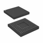 AD9129BBC
The activity of extra discounts on wholesale prices is in full swing…
Please fill in your contact information and we will send you the latest wholesale price list.





