 ChipApex | Global Electronic Components Supplier
AD9129BBCZ
Search Product
Search Post
— IC芯片 | 连接器 | 传感器 | 被动器件 —
Search productSearch post
— IC芯片 | 连接器 | 传感器 | 被动器件 —
Consult the customer manager about the wholesale price.
consultation hotline:86-132-6715-2157
email:[email protected]
Contact the product manager for consultation. One-stop consultation is available.
Do you want a lower wholesale price? Please send us your inquiry and we will reply immediately.
The AD9129BBCZ is a high-performance, single-channel, 14-bit RF digital-to-analog converter (DAC) manufactured by Analog Devices Inc. It supports data rates up to 2.85 GSPS and achieves an effective update rate of 5.7 GSPS when configured for Mix-Mode or 2× interpolation. The device utilizes a quad-switch architecture based on a 0.18 µm CMOS process, enabling direct RF synthesis in the second and third Nyquist zones up to 4.2 GHz. Key electrical parameters include a full-scale output current range of 9.5 mA to 34.4 mA, integral nonlinearity (INL) of ±1.4 LSB, and differential nonlinearity (DNL) of ±1.1 LSB. It operates from +1.8 V analog/digital supplies and −1.5 V analog supply.
Verify the specific suffix 'BBCZ' corresponds to the standard BGA package configuration as defined in the official Analog Devices ordering guide. Confirm that the required operating temperature range of -40°C to +85°C aligns with system environmental specifications. Ensure compatibility with the 160-ball CSP_BGA footprint during PCB layout planning.
Select the AD9129BBCZ over the AD9119 variant when 14-bit resolution is required for higher dynamic range applications. Consider Mix-Mode operation if RF carrier synthesis above 1.425 GHz is necessary. Evaluate power consumption at 1.3 W (at 5.7 GSPS) against thermal management capabilities. Verify interface compatibility with host FPGA/ASIC using LVDS or DHSTL standards.
The AD9129 belongs to the AD9119/AD9129 family of high-speed RF DACs. It shares the same functional block diagram and interface protocols as the 11-bit AD9119 but offers increased resolution. Both devices are designed for signal synthesis applications requiring wide bandwidth and low noise spectral density.
Public confirmed substitute part numbers are not available in the provided documentation. The AD9119 is a related component within the same family but differs in resolution (11-bit vs. 14-bit).
The AD9129 supports a DAC update rate of up to 5.7 GSPS when configured for Mix-Mode or 2× interpolation.
The quad-switch architecture enables dual-edge clocking operation, which effectively increases the DAC update rate and allows for industry-leading direct RF synthesis performance with minimal loss in output power.
The output compliance range is specified from 1.5 V to 2.5 V relative to the negative analog supply (VSSA).
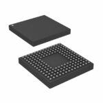 AD9129BBCZ
The activity of extra discounts on wholesale prices is in full swing…
Please fill in your contact information and we will send you the latest wholesale price list.





