 ChipApex | Global Electronic Components Supplier
AD9250BCPZRL7-250
Search Product
Search Post
— IC芯片 | 连接器 | 传感器 | 被动器件 —
Search productSearch post
— IC芯片 | 连接器 | 传感器 | 被动器件 —
Consult the customer manager about the wholesale price.
consultation hotline:86-132-6715-2157
email:[email protected]
Contact the product manager for consultation. One-stop consultation is available.
Do you want a lower wholesale price? Please send us your inquiry and we will reply immediately.
The AD9250BCPZRL7-250 is a dual-channel, 14-bit analog-to-digital converter (ADC) from Analog Devices Inc., designed for high-speed data acquisition. It supports sampling rates up to 250 MSPS with an internal voltage reference and JESD204B serial interface. The device operates on a single 1.8 V supply, consuming 711 mW at maximum speed. Key electrical parameters include a signal-to-noise ratio of 70.6 dBFS at 185 MHz input frequency and a spurious-free dynamic range of 88 dBc. It features a 48-lead LFCSP package and functions within an industrial temperature range of -40°C to +85°C.
Verify the specific ordering suffix RL7 against the manufacturer's current datasheet revision E documentation to confirm reel packaging specifications and tape-and-reel dimensions. Ensure compatibility with the intended PCB footprint for the 48-lead LFCSP package before finalizing procurement orders.
Select this component when system requirements demand dual-channel conversion at 250 MSPS with low power consumption. The integrated JESD204B interface reduces board routing complexity compared to parallel interfaces. Consider the 1.8 V supply requirement and thermal dissipation characteristics associated with the LFCSP package during the initial design phase.
This part belongs to the AD9250 family of high-speed data converters. It shares architectural similarities with other members like the AD9250-170 but offers higher throughput capabilities. The device is positioned for applications requiring compact form factors and versatile interfacing options in communication and instrumentation systems.
Direct substitutes within the same family include the AD9250-170 variant, which supports lower sampling rates. Verify pinout compatibility and electrical parameter margins when considering alternative manufacturers' dual-channel 14-bit ADCs with JESD204B outputs.
The configurable JESD204B output block supports data rates of up to 5 Gbps per lane.
An integrated duty cycle stabilizer (DCS) compensates for variations in the ADC clock duty cycle to maintain excellent performance.
No, the AD9250 includes an internal analog-to-digital converter voltage reference to simplify design considerations.
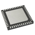 AD9250BCPZRL7-250
The activity of extra discounts on wholesale prices is in full swing…
Please fill in your contact information and we will send you the latest wholesale price list.





