 ChipApex | Global Electronic Components Supplier

SEARCH
Search Product
Search Post
— IC芯片 | 连接器 | 传感器 | 被动器件 —
Search productSearch post
— IC芯片 | 连接器 | 传感器 | 被动器件 —
Consult the customer manager about the wholesale price.
consultation hotline:86-132-6715-2157
email:[email protected]
Contact the product manager for consultation. One-stop consultation is available.
Do you want a lower wholesale price? Please send us your inquiry and we will reply immediately.
The AD9272BSVZ-40 is an octal analog front-end integrated circuit featuring eight independent channels, each comprising a low noise preamplifier (LNA), variable gain amplifier (VGA), antialiasing filter (AAF), and a 12-bit analog-to-digital converter (ADC). Designed for high-performance signal acquisition, it supports sampling rates up to 40 MSPS. The device integrates an 8x8 differential crosspoint switch to facilitate continuous wave Doppler applications. It operates with single-ended inputs and provides fully differential signal paths, optimized for dynamic range and low power consumption in compact packages.
Verify the specific speed grade suffix (-40) against the required system clock frequency. Confirm that the 100-lead TQFP package dimensions match the PCB footprint requirements. Ensure that the supply voltages (AVDD1 1.8 V, AVDD2 3.0 V, DRVDD 1.8 V) are compatible with the target power rails before procurement.
Select the AD9272BSVZ-40 when a maximum sampling rate of 40 MSPS is sufficient for the application bandwidth. Consider the -65 or -80 variants if higher throughput is required. Evaluate the power consumption profiles, noting that TGC mode consumes approximately 195 mW per channel at 40 MSPS, while CW Doppler mode reduces this significantly.
This component belongs to the AD9272 family of octal analog front ends. The -40 suffix denotes the 40 MSPS speed grade variant, distinct from the -65 and -80 grades which support higher sampling rates. All variants share the same pinout, functional block diagram, and general specifications, differing primarily in their maximum clock rate capabilities.
Direct replacements within the same family include the AD9272BSVZ-65 and AD9272BSVZ-80, which offer higher sampling rates but maintain identical pinouts and functionality.
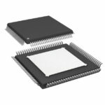 AD9272BSVZ-40

The activity of extra discounts on wholesale prices is in full swing…
Please fill in your contact information and we will send you the latest wholesale price list.





