 ChipApex | Global Electronic Components Supplier

SEARCH
Search Product
Search Post
— IC芯片 | 连接器 | 传感器 | 被动器件 —
Search productSearch post
— IC芯片 | 连接器 | 传感器 | 被动器件 —
Consult the customer manager about the wholesale price.
consultation hotline:86-132-6715-2157
email:[email protected]
Contact the product manager for consultation. One-stop consultation is available.
Do you want a lower wholesale price? Please send us your inquiry and we will reply immediately.
The AD9272BSVZ-80 is an octal analog front-end integrated circuit featuring eight independent channels, each comprising a low noise preamplifier (LNA), variable gain amplifier (VGA), antialiasing filter (AAF), and 12-bit analog-to-digital converter (ADC). It supports sampling rates up to 80 MSPS with a typical signal-to-noise ratio of 70 dB and spurious-free dynamic range of 75 dB. The device includes an 8x8 differential crosspoint switch for continuous wave Doppler applications. Power consumption is 195 mW per channel at 40 MSPS in full TGC mode. It operates over the industrial temperature range of −40°C to +85°C and is housed in a 100-lead TQFP package.
Verify the specific speed grade suffix (-80) against the manufacturer's current ordering guide to confirm availability and lead times. Ensure that the 100-lead TQFP package dimensions match the target PCB footprint requirements. Confirm power supply decoupling strategies for AVDD1, AVDD2, and DRVDD rails to maintain specified performance levels.
Select the AD9272BSVZ-80 when system requirements demand sampling rates up to 80 MSPS. Compare power dissipation characteristics against lower speed grades if thermal management is constrained. Verify that the single-ended input voltage range and PGA gain settings align with the sensor interface specifications.
This component belongs to the AD9272 family of octal ultrasound ADCs. Other variants include the AD9272BSVZ-40 and AD9272BSVZ-65, which offer lower maximum sampling rates of 40 MSPS and 65 MSPS respectively. All variants share the same pinout and functional architecture but differ in high-speed performance specifications.
Direct replacements within the same family are the AD9272BSVZ-40 and AD9272BSVZ-65. These parts are pin-compatible but operate at lower maximum clock frequencies. System timing constraints must be verified to ensure compatibility with the reduced bandwidth.
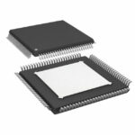 AD9272BSVZ-80

The activity of extra discounts on wholesale prices is in full swing…
Please fill in your contact information and we will send you the latest wholesale price list.







