 ChipApex | Global Electronic Components Supplier

SEARCH
Search Product
Search Post
— IC芯片 | 连接器 | 传感器 | 被动器件 —
Search productSearch post
— IC芯片 | 连接器 | 传感器 | 被动器件 —
Consult the customer manager about the wholesale price.
consultation hotline:86-132-6715-2157
email:[email protected]
Contact the product manager for consultation. One-stop consultation is available.
Do you want a lower wholesale price? Please send us your inquiry and we will reply immediately.
AD9445BSVZ-105 is listed in the Analog To Digital Converters (ADC) range at ChipApex. The manufacturer field lists Analog Devices Inc.. Its product description is IC ADC 14BIT PIPELINED 100TQFP. Review the specifications below when checking this part for your BOM.
The AD9445BSVZ-105 is a 14-bit, monolithic sampling analog-to-digital converter (ADC) with an on-chip IF sampling track-and-hold circuit. It operates at a guaranteed maximum sampling rate of 105 MSPS and requires 3.3 V and 5.0 V power supplies. The device features buffered analog inputs supporting differential full-scale input spans from 2.0 V p-p to 4.0 V p-p. Digital outputs are available in CMOS or LVDS formats compatible with ANSI-644 standards. It includes an internal reference, clock duty cycle stabilizer, and out-of-range detection.
Verify the specific speed grade suffix matches the required sampling rate. Confirm package type and temperature range alignment with system requirements. Ensure supply voltages match the specified 3.3 V and 5.0 V rails. Check for lead-free compliance if required by assembly standards.
Select this component for applications requiring high linearity and low jitter at intermediate frequencies. Consider the 105 MSPS limit when designing clock circuits. Evaluate power consumption differences between CMOS and LVDS output modes. Verify thermal management capabilities for the 100-lead TQFP/EP package.
This part belongs to the AD9445 family of high-speed ADCs from Analog Devices. It shares architectural similarities with other members but is distinguished by its 105 MSPS maximum conversion rate specification. The device is designed for base station receivers and instrumentation applications.
AD9445BSVZ-125 offers a higher 125 MSPS sampling rate with similar pinout and functionality.
The RF ENABLE pin configures the analog front end to optimize SFDR performance. For the AD9445-105, connecting it to AVDD1 is recommended for analog input frequencies above 230 MHz.
The Data Format Select (DFS) pin determines the output data format. Connecting DFS to AVDD1 selects two's complement, while connecting it to ground selects offset binary.
The AD9445BSVZ-105 has a typical aperture uncertainty (jitter) of 60 fsec rms.
Explore related parts through Data Acquisition, Integrated Circuits (ICs), all product categories, ChipApex homepage.
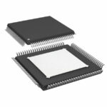 AD9445BSVZ-105

The activity of extra discounts on wholesale prices is in full swing…
Please fill in your contact information and we will send you the latest wholesale price list.




