 ChipApex | Global Electronic Components Supplier

SEARCH
Search Product
Search Post
— IC芯片 | 连接器 | 传感器 | 被动器件 —
Search productSearch post
— IC芯片 | 连接器 | 传感器 | 被动器件 —
Consult the customer manager about the wholesale price.
consultation hotline:86-132-6715-2157
email:[email protected]
Contact the product manager for consultation. One-stop consultation is available.
Do you want a lower wholesale price? Please send us your inquiry and we will reply immediately.
AD9511BCPZ-REEL7 is listed in the Clock Buffers, Drivers range at ChipApex. The manufacturer field lists Analog Devices Inc.. Its product description is IC CLK BUFFER 2:5 1.2GHZ 48LFCSP. Review the specifications below when checking this part for your BOM.
The AD9511BCPZ-REEL7 is a clock distribution integrated circuit manufactured by Analog Devices Inc. It features an on-chip PLL core, programmable dividers, and delay adjustment capabilities. The device provides five independent outputs: three LVPECL outputs supporting frequencies up to 1.2 GHz, and two outputs configurable as either LVDS (up to 800 MHz) or CMOS (up to 250 MHz). It operates from a single 3.3 V supply with a voltage range of 3.135 V to 3.465 V. The component is housed in a 48-lead LFCSP package and supports an operating temperature range of -40°C to +85°C.
Verify the REEL7 suffix indicates tape and reel packaging when sourcing. Confirm the specific lot date code and moisture sensitivity level requirements against storage guidelines. Ensure the ordering part number matches the exact electrical specifications required for the target application design.
Select this component for applications requiring subpicosecond jitter performance for data converters. Choose based on the need for mixed logic levels (LVPECL, LVDS, CMOS) within a single package. Consider the external VCO/VCXO compatibility if utilizing the PLL core for frequency synthesis rather than simple distribution.
This part belongs to the AD9511 series of clock distribution ICs. The BCPZ designation indicates a lead-free, RoHS-compliant version in a 48-lead LFCSP package. The REEL7 suffix specifies the bulk packaging format for automated assembly processes.
The maximum input frequency for both CLK1 and CLK2 differential inputs is 1.6 GHz.
No, OUT3 and OUT4 are individually selectable as either LVDS or CMOS levels; they cannot operate as different logic types simultaneously on the same pin pair.
The additive output jitter for the LVPECL outputs is typically 225 fs rms.
Explore related parts through Clock/Timing, Integrated Circuits (ICs), all product categories, ChipApex homepage.
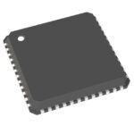 AD9511BCPZ-REEL7

The activity of extra discounts on wholesale prices is in full swing…
Please fill in your contact information and we will send you the latest wholesale price list.




