 ChipApex | Global Electronic Components Supplier
SEARCH
Search Product
Search Post
— IC芯片 | 连接器 | 传感器 | 被动器件 —
Search productSearch post
— IC芯片 | 连接器 | 传感器 | 被动器件 —
Consult the customer manager about the wholesale price.
consultation hotline:86-132-6715-2157
email:[email protected]
Contact the product manager for consultation. One-stop consultation is available.
Do you want a lower wholesale price? Please send us your inquiry and we will reply immediately.
The AD9516-0BCPZ-REEL7 is a 14-output clock generator featuring an integrated voltage-controlled oscillator (VCO) with a tuning range of 2.55 GHz to 2.95 GHz. It supports up to 2.4 GHz external VCO/VCXO inputs and accepts LVPECL, LVDS, or CMOS references up to 250 MHz. The device provides six pairs of LVPECL outputs operating to 1.6 GHz, four pairs of LVDS outputs to 800 MHz, and reconfigurable CMOS outputs to 250 MHz. Additive output jitter is specified at 225 fs rms for LVPECL and 275 fs rms for LVDS. It operates on a single 3.3 V supply within the -40°C to +85°C temperature range.
Verify the REEL7 suffix indicates tape and reel packaging when sourcing. Confirm the specific AD9516-0 variant matches the required internal VCO frequency range of 2.55 GHz to 2.95 GHz. Ensure compatibility with the 64-lead LFCSP package dimensions and moisture sensitivity level requirements during assembly.
Select this component for applications requiring subpicosecond jitter performance and multiple differential output formats. The AD9516-0 is distinct from other family members by its specific internal VCO tuning range. Consider the programmable divider ratios and fine delay adjustments available for each output pair when designing complex clock trees.
The AD9516-0 belongs to the Analog Devices AD9516 family of multi-output clock generators. This specific model integrates a high-frequency VCO optimized for low phase noise. Other variants in the series may feature different VCO ranges or external VCO dependencies, making the -0 suffix critical for identifying the correct internal oscillator specifications.
Direct substitutes include other AD9516 family members such as AD9516-1, AD9516-2, AD9516-3, and AD9516-4. Verify that the alternative variant's internal VCO frequency range and output configurations match the design requirements before substitution.
The reference inputs accept frequencies up to 250 MHz.
Yes, each LVDS output can be reconfigured as two separate 250 MHz CMOS outputs.
The additive output jitter for LVPECL outputs is 225 fs rms.
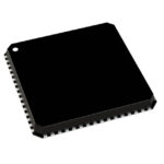 AD9516-0BCPZ-REEL7
The activity of extra discounts on wholesale prices is in full swing…
Please fill in your contact information and we will send you the latest wholesale price list.





