 ChipApex | Global Electronic Components Supplier
AD9524BCPZ
Search Product
Search Post
— IC芯片 | 连接器 | 传感器 | 被动器件 —
Search productSearch post
— IC芯片 | 连接器 | 传感器 | 被动器件 —
Consult the customer manager about the wholesale price.
consultation hotline:86-132-6715-2157
email:[email protected]
Contact the product manager for consultation. One-stop consultation is available.
Do you want a lower wholesale price? Please send us your inquiry and we will reply immediately.
The AD9524BCPZ is a low-power, multi-output clock generator and jitter cleaner featuring a dual PLL architecture with an integrated VCO. It provides six configurable differential outputs (LVPECL, LVDS, HSTL) and supports single-ended CMOS modes. The device operates from 1 MHz to 1 GHz with absolute output jitter below 200 fs at 122.88 MHz. It includes dedicated output dividers with adjustable delay, automatic synchronization on power-up, and nonvolatile EEPROM storage for configuration settings.
Verify the specific ordering suffix against the manufacturer's current data sheet to confirm package type and temperature range. Confirm that the required supply voltages (VDD3_PLL1, VDD3_PLL2, VDD3_REF, VDD3_OUT at 3.3 V and VDD1.8_OUT at 1.8 V) match the target system design before procurement.
Select this component when low phase noise and precise timing alignment are critical. Ensure the application requires an external VCXO for PLL1 reference cleanup if ultra-low jitter is needed. Verify that the available output formats (LVPECL, LVDS, HSTL, CMOS) align with the downstream device requirements.
The AD9524 belongs to Analog Devices' family of integer-N clock generators designed for high-performance wireless infrastructure. It complements other devices like the AD9522 and AD9520 by offering a specific combination of dual PLLs, integrated VCO, and flexible output configurations optimized for LTE and telecom applications.
Publicly confirmed substitute part numbers are not provided in the source material. Consult the manufacturer's official documentation for cross-reference information or updated product lifecycle status.
The integrated VCO tunes from 3.6 GHz to 4.0 GHz.
There are 63 resolution steps, each equal to half the period of the VCO output divider signal.
Yes, but using an external VCXO with PLL1 is recommended for achieving the restrictive low phase noise requirements necessary for acceptable data converter SNR performance.
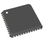 AD9524BCPZ
The activity of extra discounts on wholesale prices is in full swing…
Please fill in your contact information and we will send you the latest wholesale price list.






