 ChipApex | Global Electronic Components Supplier
AD9528BCPZ
Search Product
Search Post
— IC芯片 | 连接器 | 传感器 | 被动器件 —
Search productSearch post
— IC芯片 | 连接器 | 传感器 | 被动器件 —
Consult the customer manager about the wholesale price.
consultation hotline:86-132-6715-2157
email:[email protected]
Contact the product manager for consultation. One-stop consultation is available.
Do you want a lower wholesale price? Please send us your inquiry and we will reply immediately.
The AD9528BCPZ is a dual-stage phase-locked loop (PLL) clock generator with an integrated JESD204B/JESD204C SYSREF generator, designed for multi-device synchronization. It features 14 LVDS/HSTL outputs, with six channels supporting frequencies up to 1.25 GHz and eight channels up to 1 GHz. The device includes a two-stage PLL architecture where the first stage cleans reference jitter using an external VCXO, and the second stage utilizes an on-chip VCO tuned from 3.450 GHz to 4.025 GHz. Supply voltage ranges from 3.135 V to 3.465 V, with maximum supply current reaching 71 mA.
Verify that the component matches the exact part number AD9528BCPZ. Confirm the package type is LFCSP with 72 pins. Ensure the operating temperature range meets requirements of -40°C to +85°C. Check serial control port compatibility for SPI or I2C interfaces as needed for system integration.
Select this component when precise timing alignment across multiple devices is required. The dual PLL structure allows for low jitter performance by utilizing an external VCXO for the first stage. Ensure the application supports the required supply voltage range of 3.135 V to 3.465 V and accommodates the maximum power dissipation specifications under full load conditions.
The AD9528BCPZ belongs to the Analog Devices AD9528 family of clock generators. It is specifically engineered for systems requiring deterministic latency and synchronization, such as those adhering to the JESD204B and JESD204C standards. The 'BCPZ' suffix indicates the specific package and temperature grade configuration within the product line.
Public confirmed substitute part numbers are not available in the provided documentation. Verify pinout and electrical specifications against any potential alternative components before substitution.
The on-chip VCO tunes from 3.450 GHz to 4.025 GHz.
Six outputs (Output 0 to Output 3, Output 12, and Output 13) support maximum frequencies of 1.25 GHz.
The integrated SYSREF generator outputs single shot, N-shot, or continuous signals synchronous to the PLL1 and PLL2 outputs.
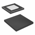 AD9528BCPZ
The activity of extra discounts on wholesale prices is in full swing…
Please fill in your contact information and we will send you the latest wholesale price list.







