 ChipApex | Global Electronic Components Supplier
AD9551BCPZ-REEL7
Search Product
Search Post
— IC芯片 | 连接器 | 传感器 | 被动器件 —
Search productSearch post
— IC芯片 | 连接器 | 传感器 | 被动器件 —
Consult the customer manager about the wholesale price.
consultation hotline:86-132-6715-2157
email:[email protected]
Contact the product manager for consultation. One-stop consultation is available.
Do you want a lower wholesale price? Please send us your inquiry and we will reply immediately.
The AD9551BCPZ-REEL7 is a multiservice clock generator manufactured by Analog Devices Inc. It utilizes a fractional-N PLL architecture with sigma-delta modulators to translate input reference frequencies into precise output signals. The device supports dual reference inputs and dual clock outputs, accommodating frequencies from 10 MHz to 900 MHz for outputs and 19.44 MHz to 806 MHz for inputs. It features pin-programmable settings for standard network rates and SPI programmability for arbitrary rational ratios. Key capabilities include holdover operation via an external crystal, hitless switchover between references, and support for forward error correction (FEC) rates. The component operates on a single 3.3 V supply within the -40°C to +85°C temperature range.
Verify the REEL7 suffix indicates tape-and-reel packaging when sourcing components. Confirm that the specific revision matches the required design specifications, as Analog Devices may update documentation without notice. Ensure compatibility with the intended serial programming interface and power supply requirements before integration.
Select this component for applications requiring precise frequency translation between disparate standard network rates. The AD9551 is suitable where jitter generation meets OC-192 high band requirements. Consider the need for dual independent outputs and the availability of pin-programmable presets versus full SPI configurability based on system complexity.
The AD9551 belongs to the Analog Devices multiservice clock generator family, designed for telecommunications infrastructure. It addresses the challenge of generating exact output frequencies from various input timing bases without bit or cycle slips. The device integrates reference conditioning, loop filters, and output drivers, simplifying the design of complex clocking networks in high-speed digital systems.
Public confirmed substitute part numbers are not available in the provided source material. Evaluate alternative clock generators based on similar fractional-N PLL architectures, output frequency ranges up to 900 MHz, and dual-reference input capabilities if direct replacement is necessary.
The device includes reference conditioning and switchover circuitry that internally synchronizes two references. If the active reference fails, it automatically switches to the backup reference with virtually no phase perturbation. If both references fail, it enters holdover mode using an external crystal.
The external crystal provides the clock source for the reference synchronization and monitoring functions. It is essential for holdover operation, allowing the device to maintain a steady output signal even when both reference inputs are unavailable.
Yes, while it offers pin-programmable presets for standard network rates, the SPI-compatible 3-wire programming interface allows users to override these settings to achieve almost any rational input-to-output frequency ratio.
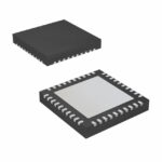 AD9551BCPZ-REEL7
The activity of extra discounts on wholesale prices is in full swing…
Please fill in your contact information and we will send you the latest wholesale price list.





