 ChipApex | Global Electronic Components Supplier
AD9553BCPZ
Search Product
Search Post
— IC芯片 | 连接器 | 传感器 | 被动器件 —
Search productSearch post
— IC芯片 | 连接器 | 传感器 | 被动器件 —
Consult the customer manager about the wholesale price.
consultation hotline:86-132-6715-2157
email:[email protected]
Contact the product manager for consultation. One-stop consultation is available.
Do you want a lower wholesale price? Please send us your inquiry and we will reply immediately.
The AD9553BCPZ is a flexible clock translator based on an integer-N phase-locked loop (PLL). It accepts input frequencies from 8 kHz to 710 MHz and generates output frequencies up to 810 MHz. The device supports LVPECL, LVDS, and CMOS outputs, with CMOS limited to 200 MHz. It features pin-programmable frequency translation ratios for standard applications and arbitrary ratios via a 3-wire SPI interface. An on-chip VCO and crystal input capability enable holdover functionality. Powered by a single 3.3 V supply (3.135 V to 3.465 V), it operates within the -40°C to +85°C temperature range in a 32-LFCSP-WQ package.
Verify the component revision matches Rev. A specifications. Confirm the package type is 32-LFCSP-WQ (5x5 mm) with an exposed pad requiring ground connection. Ensure the operating environment stays within the specified -40°C to +85°C range and supply voltage limits of 3.135 V to 3.465 V.
Select this device when flexible frequency translation between disparate clock standards is required. Use pin programming for fixed ratio applications like SONET or Ethernet. Utilize the SPI interface for custom frequency synthesis. Consider the low power consumption (<450 mW) and small footprint for space-constrained designs.
The AD9553 serves as a cost-effective replacement for high-frequency VCXOs, OCXOs, and SAW resonators. It addresses timing needs in multi-service line cards where multiple clock domains must be synchronized. The device integrates reference selection, PLL synthesis, and output buffering into a single CMOS solution.
Public confirmed substitute part numbers are not available in the provided documentation.
The CMOS output mode is limited to a maximum frequency of 200 MHz.
The AD9553 supports holdover by allowing a 25 MHz crystal resonator to be connected across the XTAL pins.
Yes, while 15 input and 52 output presets are available via pins, arbitrary ratios can be programmed using the 3-wire SPI interface.
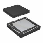 AD9553BCPZ
The activity of extra discounts on wholesale prices is in full swing…
Please fill in your contact information and we will send you the latest wholesale price list.





