 ChipApex | Global Electronic Components Supplier
AD9574BCPZ
Search Product
Search Post
— IC芯片 | 连接器 | 传感器 | 被动器件 —
Search productSearch post
— IC芯片 | 连接器 | 传感器 | 被动器件 —
Consult the customer manager about the wholesale price.
consultation hotline:86-132-6715-2157
email:[email protected]
Contact the product manager for consultation. One-stop consultation is available.
Do you want a lower wholesale price? Please send us your inquiry and we will reply immediately.
The AD9574BCPZ is a dedicated phase-locked loop (PLL) clock generator optimized for Ethernet and Gigabit Ethernet line card applications. It features a fully integrated VCO/PLL core with redundant input reference clock capability and a reference monitoring function. The device supports preset frequency translations using 19.44 MHz or 25 MHz inputs, generating outputs such as 156.25 MHz, 312.5 MHz, and others. It provides seven differential output channels supporting HSTL, LVDS, HCSL, and CMOS drive formats. Key electrical parameters include a supply voltage of 3.3 V (range 2.97 V to 3.63 V), typical power dissipation of 569 mW in a typical configuration, and operation within a temperature range of -40°C to +85°C.
Verify the specific suffix against the manufacturer's ordering guide to confirm package type and reel specifications. Confirm that the LFCSP-48 package matches the target PCB footprint. Ensure the operating environment stays within the specified -40°C to +85°C range. Check for any recent Product Change Notices (PCN) regarding assembly relocation or material updates.
Select this component when hardware-based configuration via resistors is preferred over digital control. Ensure the application requires the specific preset frequencies supported by the PPRx pin states. Verify that the required output drive formats (HSTL/LVDS/HCSL/CMOS) are available on the designated output channels. Confirm that the single 3.3 V supply constraint fits the system power architecture.
The AD9574 belongs to Analog Devices' portfolio of high-performance frequency synthesizers designed for network infrastructure. It serves as a specialized solution for deterministic clocking in high-speed serial data transmission environments. The device integrates functions typically requiring multiple discrete components, reducing board space and complexity in dense networking equipment designs.
Publicly confirmed substitute part numbers are not provided in the source documentation. Evaluate other members of the AD957x family or general-purpose clock generators if functional compatibility with the PPRx configuration scheme is not required.
Configuration is achieved through hardware strapping pins (PPR0 to PPR6). Connecting pull-up or pull-down resistors to these pins sets the internal dividers, defining the frequency translation, output functionality, and reference input behavior.
At 156.25 MHz, the device achieves 0.234 ps rms jitter (10 kHz to 10 MHz bandwidth) and 0.243 ps rms jitter (12 kHz to 20 MHz bandwidth) when using a 19.44 MHz or 25 MHz input reference.
Yes, it features redundant input reference capabilities with two independent reference inputs (REF0 and REF1). A reference monitoring function allows for quality of service status indication and switchover between sources.
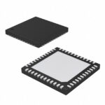 AD9574BCPZ
The activity of extra discounts on wholesale prices is in full swing…
Please fill in your contact information and we will send you the latest wholesale price list.





