 ChipApex | Global Electronic Components Supplier
AD9575ARUZLVD
Search Product
Search Post
— IC芯片 | 连接器 | 传感器 | 被动器件 —
Search productSearch post
— IC芯片 | 连接器 | 传感器 | 被动器件 —
Consult the customer manager about the wholesale price.
consultation hotline:86-132-6715-2157
email:[email protected]
Contact the product manager for consultation. One-stop consultation is available.
Do you want a lower wholesale price? Please send us your inquiry and we will reply immediately.
The AD9575ARUZLVD is a dual-output network clock generator featuring an integrated VCO/PLL core optimized for low jitter performance. It operates on a single 3.3 V supply within the -40°C to +85°C temperature range and utilizes a 16-lead TSSOP package. The device accepts external crystals at 19.44 MHz, 25 MHz, or 25.78125 MHz to generate output frequencies up to 312.5 MHz via pin-selectable divide ratios. This specific variant provides LVDS output format with typical rms jitter of 0.39 ps (12 kHz to 20 MHz) at 156.25 MHz.
Verify the ordering suffix LVD confirms the LVDS output configuration against the manufacturer's Ordering Guide. Confirm the package option RU-16 matches the required 16-lead TSSOP footprint. Ensure the temperature grade A covers the operational environment requirements of -40°C to +85°C.
Select this component when LVDS signaling is required for the primary clock output. Compare jitter specifications across different output frequencies if operating at 106.25 MHz or 312.5 MHz. Verify that the internal VCO range (2.488 GHz to 2.55 GHz) supports the desired frequency translation from the selected crystal reference.
The AD9575 series includes variants with different output formats. The ARUZPEC suffix denotes LVPECL outputs, while the ARUZLVD suffix specifies LVDS outputs. Both share the same PLL architecture and package dimensions but differ in output buffer design and termination requirements.
The AD9575ARUZPEC serves as a functional alternative if LVPECL outputs are acceptable instead of LVDS. No other direct cross-model replacements are documented in the provided datasheet.
The maximum output frequency is 312.5 MHz.
No, the AD9575 features an integrated third-order loop filter, eliminating the need for external components.
Output frequencies are determined by the logic states of the SEL0 and SEL1 pins, which configure the feedback and output divider ratios.
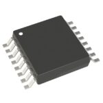 AD9575ARUZLVD
The activity of extra discounts on wholesale prices is in full swing…
Please fill in your contact information and we will send you the latest wholesale price list.






