 ChipApex | Global Electronic Components Supplier
SEARCH
Search Product
Search Post
— IC芯片 | 连接器 | 传感器 | 被动器件 —
Search productSearch post
— IC芯片 | 连接器 | 传感器 | 被动器件 —
Consult the customer manager about the wholesale price.
consultation hotline:86-132-6715-2157
email:[email protected]
Contact the product manager for consultation. One-stop consultation is available.
Do you want a lower wholesale price? Please send us your inquiry and we will reply immediately.
The AD974BRS is a four-channel, 16-bit analog-to-digital converter (ADC) data acquisition system manufactured by Analog Devices Inc. It operates from a single +5 V supply and supports throughput rates up to 200 kSPS. The device integrates an input multiplexer, a high-speed sampling ADC, and a +2.5 V reference. It accommodates analog input ranges of –10 V, 0 V to +4 V, or 0 V to +5 V. The component features a serial interface for efficient data transfer with minimal interconnects. It is housed in a 28-lead SSOP package and specified for operation between –40°C and +85°C.
Verify the specific grade (A or B) required for linearity and dynamic range specifications. Confirm the package type matches the design footprint, as the AD974 series includes DIP, SOIC, and SSOP variants. Ensure the selected part number corresponds to the desired temperature range and performance grade before ordering.
Select the AD974BRS when a compact SSOP package is required for the application. Choose this model over other grades if the A-grade specifications for Integral Nonlinearity Error (–3.0 LSB) and Signal-to-(Noise+Distortion) (83 dB) are sufficient. Verify that the serial interface timing aligns with the host microcontroller capabilities.
The AD974BRS belongs to the AD974 family of data acquisition systems. This family combines multiplexed inputs, ADC conversion, and reference generation on a single BiCMOS chip. Other variants include the AD974AN/BN (DIP) and AD974AR/BR (SOIC), offering different packaging options while maintaining identical electrical characteristics for their respective grades.
Direct replacements within the same family include the AD974ARS (A-grade SSOP) or AD974BR (B-grade SOIC). Ensure the substitute maintains the required package outline and pin compatibility. Verify that the thermal resistance and power dissipation limits of the alternative package meet the system's thermal design constraints.
The device supports three input ranges: –10 V (bipolar), 0 V to +4 V, and 0 V to +5 V (unipolar).
The EXT/INT pin determines the clock source. Tying it low enables the internal data clock, while tying it high allows synchronization with an external clock signal applied to the DATACLK pin.
When the PWRD pin is set to a logic HIGH, the power consumption is reduced to a maximum of 50 mW.
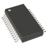 AD974BRS
The activity of extra discounts on wholesale prices is in full swing…
Please fill in your contact information and we will send you the latest wholesale price list.





