 ChipApex | Global Electronic Components Supplier
SEARCH
Search Product
Search Post
— IC芯片 | 连接器 | 传感器 | 被动器件 —
Search productSearch post
— IC芯片 | 连接器 | 传感器 | 被动器件 —
Consult the customer manager about the wholesale price.
consultation hotline:86-132-6715-2157
email:[email protected]
Contact the product manager for consultation. One-stop consultation is available.
Do you want a lower wholesale price? Please send us your inquiry and we will reply immediately.
The AD9830ASTZ is a complete Direct Digital Synthesis (DDS) device integrating a numerically controlled oscillator, sine look-up table, and 10-bit digital-to-analog converter on a single CMOS chip. It supports clock rates up to 50 MHz with frequency accuracy of one part in 4 billion. The device features parallel loading via a microprocessor interface, phase and frequency modulation capabilities, and a power-down option. Operating on a +5 V supply, it consumes 250 mW and delivers a spurious-free dynamic range of 72 dB. The component is housed in a 48-pin QFP package.
Verify the specific suffix 'ASTZ' against the manufacturer's official documentation to confirm the industrial temperature grade (-40°C to +85°C) and lead-free packaging status. Ensure the parallel interface requirements match the system design, as this model does not support serial communication protocols found in other variants within the same product family.
Select this component when a high-speed DDS solution with parallel interface compatibility is required. The 50 MHz maximum clock rate and 10-bit resolution are suitable for applications demanding precise frequency control. Consider the 48-pin QFP footprint during PCB layout planning to ensure adequate spacing for analog and digital ground separation.
The AD9830 belongs to Analog Devices' series of complete DDS synthesizers. Unlike serial-interface models such as the AD9833 or AD9834, this variant utilizes a parallel bus for data transfer. It shares core architectural elements like the 32-bit phase accumulator with other members but differs in interface speed and pin count.
The AD9831ASTZ offers similar functionality but operates with a lower maximum clock frequency of 25 MHz. Both devices utilize the 48-pin LQFP package and parallel interface, though electrical specifications and performance metrics differ significantly between the two models.
The full-scale current is determined by connecting an external resistor (RSET) between the FS ADJUST pin and AGND. The relationship is defined by IOUTFULL-SCALE = 16 * VREFIN / RSET.
The FSELECT pin controls which frequency register (FREQ0 or FREQ1) is used by the phase accumulator. It allows for frequency switching without phase discontinuity.
The AD9830 contains four 12-bit phase offset registers (PHASE0 through PHASE3), selectable via the PSEL0 and PSEL1 inputs.
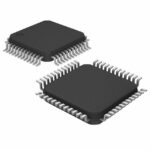 AD9830ASTZ
The activity of extra discounts on wholesale prices is in full swing…
Please fill in your contact information and we will send you the latest wholesale price list.





