 ChipApex | Global Electronic Components Supplier
SEARCH
Search Product
Search Post
— IC芯片 | 连接器 | 传感器 | 被动器件 —
Search productSearch post
— IC芯片 | 连接器 | 传感器 | 被动器件 —
Consult the customer manager about the wholesale price.
consultation hotline:86-132-6715-2157
email:[email protected]
Contact the product manager for consultation. One-stop consultation is available.
Do you want a lower wholesale price? Please send us your inquiry and we will reply immediately.
The AD9833SRMZ-EP-RL7 is an Enhanced Product programmable waveform generator from Analog Devices Inc., designed for defense and aerospace applications. It operates within a supply voltage range of 2.3 V to 5.5 V and supports an operating temperature range of −55°C to +125°C. The device features a 10-bit DAC with a maximum update rate of 25 MSPS, delivering a typical signal-to-noise ratio (SNR) of 60 dB at a 25 MHz clock frequency. It utilizes a 28-bit frequency register to achieve high resolution, such as 0.1 Hz at a 25 MHz reference clock. Power consumption is typically 12.65 mW at 3 V, with a low-power sleep mode reducing current draw to 0.5 mA when the DAC is powered down.
Verify that the component matches the specific Enhanced Product (EP) designation required for your project. Confirm the package option is the 10-Lead MSOP (RM-10) and check the branding code DMR on the device surface. Ensure the ordering suffix -RL7 corresponds to the tape and reel packaging format needed for your assembly line. Cross-reference the manufacturer part number against official Analog Devices documentation to confirm authenticity and revision status.
Select this component if the application requires operation in extreme temperatures ranging from −55°C to +125°C. It is suitable for systems needing a low-power waveform generator with digital programmability. Verify that the 10-bit resolution and 25 MSPS update rate meet the signal fidelity requirements. Ensure the design accommodates the 2.3 V to 5.5 V supply voltage range and integrates the necessary serial communication logic for the 3-wire interface.
This part belongs to the AD9833 family of direct digital synthesizers. The SRMZ-EP variant specifically denotes the Enhanced Product grade, which offers higher reliability specifications compared to standard commercial versions. It is manufactured by Analog Devices Inc. and is intended for use in critical systems where extended temperature ranges and controlled production sites are mandatory.
Standard AD9833 variants do not support the −55°C to +125°C temperature range or the enhanced product controls. Direct substitutes must be verified against the AD9833-EP datasheet for pin compatibility and electrical performance within the specified military-grade environment.
In low-power sleep mode with the DAC powered down and the master clock running, the current consumption is typically 0.5 mA.
The MCLK pin serves as the digital clock input. DDS output frequencies are expressed as a binary fraction of the MCLK frequency, determining output accuracy and phase noise.
The COMP pin is the DAC bias pin used for decoupling the DAC bias voltage to ensure stable analog output performance.
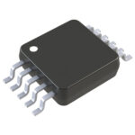 AD9833SRMZ-EP-RL7
The activity of extra discounts on wholesale prices is in full swing…
Please fill in your contact information and we will send you the latest wholesale price list.





