 ChipApex | Global Electronic Components Supplier
SEARCH
Search Product
Search Post
— IC芯片 | 连接器 | 传感器 | 被动器件 —
Search productSearch post
— IC芯片 | 连接器 | 传感器 | 被动器件 —
Consult the customer manager about the wholesale price.
consultation hotline:86-132-6715-2157
email:[email protected]
Contact the product manager for consultation. One-stop consultation is available.
Do you want a lower wholesale price? Please send us your inquiry and we will reply immediately.
The AD9841AJST is a complete analog signal processor for CCD applications, featuring a single-channel architecture designed to sample and condition outputs of interlaced and progressive scan area CCD arrays. It operates from a single 3 V power supply with typical power consumption of 78 mW. The device includes an input clamp, correlated double sampler (CDS), Pixel Gain Amplifier (PxGA), variable gain amplifier (VGA), black level clamp, and a 10-bit A/D converter. It supports a maximum clock rate of 20 MHz and utilizes a 3-wire serial digital interface for register programming.
Verify the specific ordering suffix 'JST' against the manufacturer's current documentation to confirm package type and temperature range specifications. Ensure compatibility with existing system designs regarding the 48-lead LQFP footprint and 3 V single-supply requirements before finalizing procurement decisions.
Select this component for systems requiring integrated CCD signal processing with a 10-bit ADC resolution. Consider the AD9842A variant if 12-bit resolution is required instead. Verify that the design accommodates the 48-lead LQFP package dimensions and thermal characteristics specified in the datasheet.
The AD9841AJST belongs to the AD9841A/AD9842A family of complete 20 MSPS CCD signal processors manufactured by Analog Devices. These devices are designed to handle the signal chain requirements for CCD sensors, combining analog front-end functions with digital control interfaces in a compact package.
The AD9842AJST is a direct functional substitute within the same family, differing only in ADC resolution (12-bit vs. 10-bit). No other cross-model replacements are confirmed in the provided documentation.
The maximum clock rate supported by the AD9841AJST is 20 MHz.
Internal registers are programmed through a 3-wire serial digital interface using SCK, SL, and SDATA pins.
The typical power consumption in normal operation mode is 78 mW when operating at a 3.0 V supply.
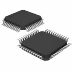 AD9841AJST
The activity of extra discounts on wholesale prices is in full swing…
Please fill in your contact information and we will send you the latest wholesale price list.





