 ChipApex | Global Electronic Components Supplier
SEARCH
Search Product
Search Post
— IC芯片 | 连接器 | 传感器 | 被动器件 —
Search productSearch post
— IC芯片 | 连接器 | 传感器 | 被动器件 —
Consult the customer manager about the wholesale price.
consultation hotline:86-132-6715-2157
email:[email protected]
Contact the product manager for consultation. One-stop consultation is available.
Do you want a lower wholesale price? Please send us your inquiry and we will reply immediately.
The AD9852ASTZ is a complete Direct Digital Synthesis (DDS) digital synthesizer manufactured by Analog Devices Inc. It features a 300 MHz internal clock rate and dual integrated 12-bit D/A converters. The device supports FSK, BPSK, PSK, chirp, and AM operations with an ultrahigh speed comparator exhibiting 3 ps rms jitter. It provides excellent dynamic performance, achieving 80 dB SFDR at 100 MHz output. Key specifications include a 4× to 20× programmable reference clock multiplier, dual 48-bit programmable frequency registers, and dual 14-bit programmable phase offset registers. It operates on a single 3.3 V supply within the -40°C to +85°C temperature range.
Verify the specific suffix ASTZ confirms the 200 MHz maximum clock frequency variant, distinct from the ASVZ 300 MHz version. Confirm package type matches LQFP-80 requirements. Ensure thermal management guidelines are followed due to exposed pad design. Check RoHS compliance status against current manufacturing revisions.
Select this component when a 200 MHz maximum system clock is sufficient for the application. Compare against AD9852ASVZ if higher frequency operation up to 300 MHz is required. Consider the 80-lead LQFP package constraints and thermal dissipation needs. Verify interface compatibility with serial or parallel programming requirements.
The AD9852ASTZ belongs to the AD9852 series of DDS synthesizers. It is pin-for-pin compatible with the AD9854 single-tone synthesizer. The ASTZ suffix denotes the industrial temperature grade (-40°C to +85°C) and the 200 MHz maximum clock frequency specification. It utilizes 0.35 μm CMOS technology.
AD9852ASVZ offers identical functionality but supports a higher maximum clock frequency of 300 MHz. AD9854 is pin-compatible but designed as a single-tone synthesizer without the dual-channel capabilities of the AD9852.
The primary difference is the maximum internal system clock frequency. The AD9852ASTZ is rated for a maximum of 200 MHz, while the AD9852ASVZ supports up to 300 MHz. Both share the same package and pinout.
The device includes a programmable 4× to 20× REFCLK multiplier that can generate the internal system clock from a lower frequency external reference clock. Direct 300 MHz clocking is also supported via single-ended or differential inputs.
It supports FSK, BPSK, PSK, chirp, and AM operations. Single-pin interfaces are provided for FSK and BPSK data, while PSK capability is available via the I/O interface.
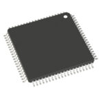 AD9852ASTZ
The activity of extra discounts on wholesale prices is in full swing…
Please fill in your contact information and we will send you the latest wholesale price list.





