 ChipApex | Global Electronic Components Supplier
SEARCH
Search Product
Search Post
— IC芯片 | 连接器 | 传感器 | 被动器件 —
Search productSearch post
— IC芯片 | 连接器 | 传感器 | 被动器件 —
Consult the customer manager about the wholesale price.
consultation hotline:86-132-6715-2157
email:[email protected]
Contact the product manager for consultation. One-stop consultation is available.
Do you want a lower wholesale price? Please send us your inquiry and we will reply immediately.
The AD9912ABCPZ is a Direct Digital Synthesizer (DDS) featuring an integrated 14-bit digital-to-analog converter (DAC). It operates with an internal clock speed of 1 GSPS, supporting direct output frequencies up to 400 MHz. The device utilizes a 48-bit frequency tuning word (FTW), enabling frequency resolution down to 4 μHz. Power supplies include DVDD and AVDD at 1.8 V, and DVDD_I/O and AVDD3 at 3.3 V. It functions within an industrial temperature range of -40°C to +85°C and is housed in a 64-lead LFCSP package.
Verify the component against official Analog Devices documentation to confirm pinout compatibility and electrical specifications. Ensure that the serial I/O control interface matches the system requirements. Check for moisture sensitivity handling procedures prior to assembly. Confirm that the thermal resistance characteristics align with the target PCB layout design.
Select this component when precise frequency agility and low phase noise are required. The integrated DDS architecture allows for rapid frequency hopping without external synthesizers. Consider the available HSTL and CMOS output drivers for different interface voltage levels. Evaluate the power consumption profiles across various operating modes to optimize system efficiency.
This part belongs to the AD9912 series of Direct Digital Synthesizers from Analog Devices. It shares core architectural features with other members of the family but is distinguished by its specific packaging and operational parameters. The AD9912ABCPZ variant provides a robust solution for applications demanding high spectral purity and flexible clock generation capabilities.
AD9912
The theoretical upper bound is 50% of the sampling clock frequency (fs), though a practical limit of 40% fs is recommended to accommodate reconstruction filter selectivity.
It accepts flexible system clock inputs via crystal or external reference clock, utilizing an on-chip low noise PLL multiplier to generate higher frequencies from lower input rates.
The FDBK_IN inputs allow the filtered DAC output signal to be fed back into the chip for further processing through the output circuitry, such as the HSTL or CMOS drivers.
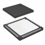 AD9912ABCPZ
The activity of extra discounts on wholesale prices is in full swing…
Please fill in your contact information and we will send you the latest wholesale price list.





