ChipApex | Global Electronic Components Supplier
ADA4098-1BUJZ-RL7
Search Product
Search Post
— IC芯片 | 连接器 | 传感器 | 被动器件 —
Search productSearch post
— IC芯片 | 连接器 | 传感器 | 被动器件 —
Consult the customer manager about the wholesale price.
consultation hotline:86-132-6715-2157
email:[email protected]
Contact the product manager for consultation. One-stop consultation is available.
Do you want a lower wholesale price? Please send us your inquiry and we will reply immediately.
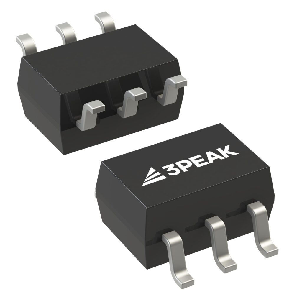
The ADA4098-1BUJZ-RL7 is a single-channel, precision operational amplifier manufactured by Analog Devices Inc. It features an ultrawide common-mode input range extending from −VS to +VS + 70 V and supports supply voltages up to 50 V. The device provides a gain-bandwidth product of 1.05 MHz and a slew rate of 0.85 V/µs. Key electrical specifications include a maximum input offset voltage of ±35 µV (B grade) and low power consumption of 165 µA per channel. It operates within a temperature range of −55°C to +150°C and utilizes a 6-lead TSOT package.
Verify the specific B-grade or H-grade performance requirements against the datasheet tables before ordering. Confirm that the 6-lead TSOT package aligns with the PCB footprint design. Ensure the application environment stays within the specified absolute maximum ratings to prevent permanent damage. Check for any required external components for stability when driving capacitive loads.
Select this component for applications requiring precision amplification where the input signal exceeds the positive supply voltage. The low offset voltage and drift make it suitable for high-accuracy measurements. Consider the thermal resistance and power dissipation limits if operating near the upper temperature extremes. Verify that the shutdown pin logic levels match the control system interface.
This part belongs to the ADA4098 family of robust, precision op amps designed for demanding industrial environments. The single-channel configuration distinguishes it from the dual-channel ADA4098-2. It is engineered to handle overvoltage conditions and harsh electrical noise while maintaining signal integrity.
Direct substitutes within the same family include the ADA4098-2 for dual-channel requirements. Other Analog Devices precision amplifiers may serve as alternatives if Over-The-Top capability is not strictly necessary.
The inputs are protected against temporary excursions down to −20 V relative to the −VS pin.
The device enters Over-The-Top mode, utilizing a secondary input stage to maintain operation without phase reversal.
Assert the SHDN pin high, specifically to a voltage greater than −VS + 1.5 V, to place the amplifier in a low-power shutdown state.
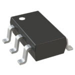 ADA4098-1BUJZ-RL7
The activity of extra discounts on wholesale prices is in full swing…
Please fill in your contact information and we will send you the latest wholesale price list.