ChipApex | Global Electronic Components Supplier
ADA4099-2BRZ
Search Product
Search Post
— IC芯片 | 连接器 | 传感器 | 被动器件 —
Search productSearch post
— IC芯片 | 连接器 | 传感器 | 被动器件 —
Consult the customer manager about the wholesale price.
consultation hotline:86-132-6715-2157
email:[email protected]
Contact the product manager for consultation. One-stop consultation is available.
Do you want a lower wholesale price? Please send us your inquiry and we will reply immediately.
The ADA4099-2BRZ is a dual precision operational amplifier from Analog Devices, featuring Over-The-Top input capability and rail-to-rail output. It operates on supply voltages ranging from 3.15 V to 50 V with a typical gain-bandwidth product of 8 MHz and a slew rate of 5.5 V/µs. The device offers low input offset voltage (±40 µV max) and drift (±0.4 µV/°C max), along with low noise density of 7 nV/√Hz at 100 Hz. It includes a low-power shutdown function drawing a maximum of 20 µA. The component is housed in an 8-lead SOIC package and supports an extended operating temperature range of -55°C to +150°C.
Verify the specific grade (B or H) required for your application, as performance specifications such as offset voltage and operating temperature range differ between grades. Confirm that the 8-lead SOIC_N package matches your PCB footprint requirements. Ensure proper ESD handling procedures are followed during assembly due to the sensitivity of the CMOS input stages. Cross-reference the datasheet revision A specifications against your design timeline to account for any parameter updates.
Select this component when high-voltage signal detection above the positive supply rail is necessary without external level shifting. The dual-channel configuration is suitable for differential sensing or dual-loop control systems requiring matched characteristics. Consider the thermal resistance of the SOIC package if driving significant load currents near the upper temperature limits. The low noise density makes it appropriate for precision measurement circuits where signal integrity is critical.
This part belongs to the ADA4099 family of robust, precision operational amplifiers designed for demanding industrial environments. The dual-channel variant shares core architectural features with the single-channel ADA4099-1 but provides two independent amplifiers in a compact 8-lead package. The family emphasizes Over-The-Top functionality, allowing inputs to exceed the positive supply voltage while maintaining precision and stability.
Direct functional substitutes within the same package include other dual-channel variants from the ADA4099 series, such as the ADA4099-2ARMZ (MSOP) or ADA4099-2BCPZ (LFCSP), provided pin compatibility and thermal profiles meet design constraints. Verify that alternative parts support the required Over-The-Top voltage range and shutdown logic levels.
When the common-mode input voltage exceeds +VS by more than 1.5 V, the internal circuitry switches to a common base input pair. This causes the input bias current to increase significantly, typically reaching approximately 82.5 µA, compared to less than 4 nA in the standard operating region.
When the SHDNx pins are asserted high (above −VS + 1.5 V), the amplifier enters a low-power shutdown state. In this condition, the output impedance becomes very high, effectively disconnecting the output driver from the load to minimize power consumption.
Yes, the inputs are protected against temporary voltage excursions. The device can tolerate differential input voltages up to ±80 V without sustaining damage, thanks to internal protection resistors and diodes integrated into the input stage.
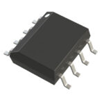 ADA4099-2BRZ
The activity of extra discounts on wholesale prices is in full swing…
Please fill in your contact information and we will send you the latest wholesale price list.