 ChipApex | Global Electronic Components Supplier
SEARCH
Search Product
Search Post
— IC芯片 | 连接器 | 传感器 | 被动器件 —
Search productSearch post
— IC芯片 | 连接器 | 传感器 | 被动器件 —
Consult the customer manager about the wholesale price.
consultation hotline:86-132-6715-2157
email:[email protected]
Contact the product manager for consultation. One-stop consultation is available.
Do you want a lower wholesale price? Please send us your inquiry and we will reply immediately.
The ADA4411-3 is an integrated triple video filter and buffer designed for RGB, HD/SD, YPbPr, and YUV signals. It features sixth-order adjustable filters with selectable cutoff frequencies of 36 MHz, 18 MHz, or 9 MHz via logic pins. The device includes 2:1 multiplexers on all inputs, variable throughput gain (×2 or ×4), and a DC output offset adjust range of ±0.5 V input-referred. Operating on a single +5 V or dual ±5 V supply, it delivers rail-to-rail outputs capable of swinging 4.5 V p-p. Quiescent power consumption is typically 265 mW across three channels, reducible to 15 μA current draw via the disable feature.
Verify the specific package variant against the ordering guide, as suffixes may indicate reel or tube packaging configurations. Confirm that the logic levels for control pins align with the system's TTL or CMOS standards. Ensure thermal management meets the junction temperature limits specified in the absolute maximum ratings during high-load operations.
Select this component when designing systems requiring simultaneous filtering and buffering for multiple video components. Evaluate the required cutoff frequency combinations based on the target video standard, such as SD or HD resolutions. Consider the power supply architecture, as single-supply designs require careful DC offset management to maintain signal integrity above the negative rail.
This device belongs to Analog Devices' family of integrated video solutions, specifically targeting high-performance analog signal processing for consumer electronics. It consolidates filtering, buffering, and multiplexing functions into a single 24-lead QSOP package, reducing board space compared to discrete implementations. The design supports extended industrial temperature ranges for robust deployment in various environments.
The ADA4412-3ARQZ serves as a functional substitute within the same product family, offering similar integrated triple video filtering capabilities.
The output DC offset is controlled differentially by applying voltages to the LEVEL1 and LEVEL2 inputs. The resulting offset voltage equals the difference between these inputs multiplied by the selected throughput gain.
Pulling the DISABLE pin to the positive supply voltage activates the power-down mode, reducing quiescent current to approximately 15 μA. When not disabled, this pin must be connected to ground to serve as the reference for other logic inputs.
Yes, each output buffer can drive two ac-coupled or dc-coupled 75 Ω source-terminated loads without requiring a separate external buffer stage.
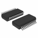 ADA4411-3ARQZ
The activity of extra discounts on wholesale prices is in full swing…
Please fill in your contact information and we will send you the latest wholesale price list.







