ChipApex | Global Electronic Components Supplier
ADA4505-1ACBZ-RL
Search Product
Search Post
— IC芯片 | 连接器 | 传感器 | 被动器件 —
Search productSearch post
— IC芯片 | 连接器 | 传感器 | 被动器件 —
Consult the customer manager about the wholesale price.
consultation hotline:86-132-6715-2157
email:[email protected]
Contact the product manager for consultation. One-stop consultation is available.
Do you want a lower wholesale price? Please send us your inquiry and we will reply immediately.
The ADA4505-1ACBZ-RL is a single-channel micropower operational amplifier from Analog Devices, featuring rail-to-rail input and output swings. It operates on a single supply of 1.8 V to 5 V or dual supplies of ±0.9 V to ±2.5 V. Key electrical parameters include a maximum offset voltage of 3 mV, typical input bias current of 0.5 pA, and supply current of 10 μA per amplifier. The device offers a gain-bandwidth product of 50 kHz, slew rate of 6 mV/µs, and minimum PSRR of 100 dB.
Verify the specific package type and tape-and-reel configuration against the official ordering guide before procurement. Confirm temperature range specifications match the application environment requirements. Ensure compatibility with existing PCB footprints for the WLCSP package. Check for any recent revision updates in the datasheet that may affect pinout or electrical characteristics.
Select this component for applications requiring high precision in low-voltage, battery-powered environments. The zero crossover distortion feature makes it suitable for signals swinging across the entire supply range. Consider the 6-ball WLCSP package for space-constrained designs. Evaluate the trade-off between the low bandwidth and the ultra-low power consumption based on system speed requirements.
This part belongs to the ADA4505 family of micropower amplifiers, which includes single (ADA4505-1), dual (ADA4505-2), and quad (ADA4505-4) variants. The family shares core technologies such as the charge pump-based input stage and CMOS architecture. It is designed to address errors caused by battery voltage decay and rail-to-rail input distortion in portable instrumentation.
Public confirmed substitute part numbers are not available in the provided documentation. Designers should consult the manufacturer's selection guide for alternative devices within the zero crossover distortion portfolio, such as the AD8505 series, while verifying pinout and electrical parameter compatibility.
It uses an on-chip charge pump to power the input differential pair, allowing the input voltage to vary from one supply extreme to the other without the need for a second differential pair that causes distortion.
The typical input bias current is 0.5 pA, which remains very low across the operating temperature range.
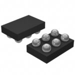 ADA4505-1ACBZ-RL
The activity of extra discounts on wholesale prices is in full swing…
Please fill in your contact information and we will send you the latest wholesale price list.