ChipApex | Global Electronic Components Supplier
ADA4897-2ARMZ
Search Product
Search Post
— IC芯片 | 连接器 | 传感器 | 被动器件 —
Search productSearch post
— IC芯片 | 连接器 | 传感器 | 被动器件 —
Consult the customer manager about the wholesale price.
consultation hotline:86-132-6715-2157
email:[email protected]
Contact the product manager for consultation. One-stop consultation is available.
Do you want a lower wholesale price? Please send us your inquiry and we will reply immediately.
The ADA4897-2 is a dual-channel, unity-gain stable, low noise, rail-to-rail output, high speed voltage feedback amplifier manufactured by Analog Devices. It features a quiescent current of 3 mA per amplifier and operates within a wide supply voltage range of 3 V to 10 V. The device utilizes a proprietary SiGe bipolar process to achieve a -3 dB bandwidth of 230 MHz at G = +1 and a slew rate of 120 V/μs. It settles to 0.1% in 45 ns with an input offset voltage maximum of 500 μV. The component includes dedicated disable pins for each channel and is housed in a 10-lead MSOP package.
Verify the specific package configuration and pinout compatibility before integration. Confirm that the disable logic levels align with the system control voltages. Ensure thermal management meets the junction temperature limits specified in the datasheet. Check for any recent revision updates that may affect parameter tolerances or ordering suffixes.
Select this component when dual-channel operation is required alongside low noise and high speed characteristics. The integrated disable feature offers power management benefits over non-disable variants. Consider the 10-lead MSOP package constraints regarding PCB layout and thermal dissipation compared to other package options in the series.
This part belongs to the ADA4896-2/ADA4897-1/ADA4897-2 family of low noise, rail-to-rail output amplifiers. It shares core electrical specifications with the ADA4896-2 and ADA4897-1 but differs in channel count and packaging. The ADA4897-2 specifically provides two channels in a 10-lead MSOP format, distinguishing it from the single-channel ADA4897-1.
The ADA4896-2 serves as a dual-channel alternative in different packages. The ADA4897-1 is a single-channel equivalent with identical electrical performance but requires separate components for dual-channel designs. Verify pinout differences when substituting between these family members.
The ADA4897-2 includes two separate disable pins, one for each channel. Driving the pin below the threshold voltage disables the respective amplifier, reducing quiescent current significantly.
The maximum input offset voltage is specified as 500 μV across the operating temperature range.
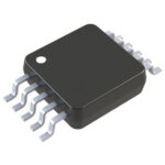 ADA4897-2ARMZ
The activity of extra discounts on wholesale prices is in full swing…
Please fill in your contact information and we will send you the latest wholesale price list.