 ChipApex | Global Electronic Components Supplier
SEARCH
Search Product
Search Post
— IC芯片 | 连接器 | 传感器 | 被动器件 —
Search productSearch post
— IC芯片 | 连接器 | 传感器 | 被动器件 —
Consult the customer manager about the wholesale price.
consultation hotline:86-132-6715-2157
email:[email protected]
Contact the product manager for consultation. One-stop consultation is available.
Do you want a lower wholesale price? Please send us your inquiry and we will reply immediately.
The ADA4932-2YCPZ-RL is a dual-channel, low-power differential ADC driver manufactured by Analog Devices Inc. It operates within a supply range of +3 V to ±5 V and features a −3 dB small-signal bandwidth of 560 MHz at unity gain. The device provides a slew rate of 2800 V/µs and a fast settling time of 9 ns to 0.1%. It delivers high linearity with an SFDR of 100 dB at 10 MHz and 90 dB at 20 MHz. Input voltage noise is specified at 3.6 nV/√Hz, with a typical input offset voltage of ±0.5 mV. Each amplifier channel consumes approximately 9.6 mA of quiescent current.
Verify that the ordering suffix matches the required reel quantity and tape-and-reel specifications. Confirm the package type corresponds to the 24-lead LFCSP-WQ variant. Ensure the temperature grade aligns with the industrial operating range of −40°C to +105°C. Cross-reference the manufacturer part number against official distributor catalogs to validate authenticity and revision status before procurement.
Select this component when driving high-performance ADCs requiring differential inputs from single-ended sources. The dual-channel design is suitable for applications needing two independent signal paths in a compact footprint. Consider the adjustable output common-mode voltage feature for interfacing with various ADC input ranges. Evaluate power consumption constraints, as the device offers low quiescent current relative to its high-speed performance capabilities.
The ADA4932-2 serves as the dual-channel counterpart to the ADA4932-1, succeeding the AD8132 family. It integrates two identical differential amplifier channels within a single 24-lead LFCSP-WQ package. This integration facilitates balanced PCB layout and minimizes board space compared to discrete solutions. The device maintains compatibility with standard feedback networks while offering improved dynamic performance and lower power consumption than previous generations.
The ADA4932-1 is the single-channel equivalent within the same series. Designers replacing older AD8132 units should verify pinout compatibility and thermal characteristics. Ensure that the replacement part meets the specific bandwidth and noise requirements of the original application circuit.
The internal common-mode feedback loop forces the outputs to remain highly balanced over a wide frequency range, ensuring signals are equal in amplitude and exactly 180° out of phase without relying on tightly matched external resistors.
The VOCM pin allows the user to adjust the output common-mode voltage. The internal feedback loop forces the output common-mode level to match the voltage applied to this pin, enabling alignment with specific ADC input requirements.
Yes, the device can be configured for gains less than one using the external four-resistor feedback network, providing flexibility for attenuation applications.
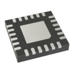 ADA4932-2YCPZ-RL
The activity of extra discounts on wholesale prices is in full swing…
Please fill in your contact information and we will send you the latest wholesale price list.







