ChipApex | Global Electronic Components Supplier
ADA4950-1YCPZ-R2
Search Product
Search Post
— IC芯片 | 连接器 | 传感器 | 被动器件 —
Search productSearch post
— IC芯片 | 连接器 | 传感器 | 被动器件 —
Consult the customer manager about the wholesale price.
consultation hotline:86-132-6715-2157
email:[email protected]
Contact the product manager for consultation. One-stop consultation is available.
Do you want a lower wholesale price? Please send us your inquiry and we will reply immediately.
The ADA4950-1YCPZ-R2 is a low-power, selectable gain differential ADC driver manufactured by Analog Devices Inc. It operates within a supply range of +3 V to ±5 V and features an operating temperature range from −40°C to +105°C. The device provides selectable differential gains of 1, 2, and 3 via internal feedback networks. Key performance metrics include a small-signal bandwidth of 750 MHz at G = 1, a slew rate of 2900 V/µs, and a quiescent current of 9.5 mA per amplifier. It utilizes a 16-lead LFCSP package.
Verify the specific ordering suffix YCPZ-R2 against the manufacturer's official documentation to confirm reel packaging and tape specifications. Ensure compatibility with the required PCB footprint for the 16-lead LFCSP package. Confirm that the selected component meets the necessary thermal resistance requirements for the intended application environment.
Select this component when driving high-performance ADCs requiring single-ended-to-differential or differential-to-differential conversion. Consider the adjustable output common-mode voltage feature for precise input matching. Evaluate the power consumption of 9.5 mA per amplifier against system constraints. Verify that the 750 MHz bandwidth meets the signal frequency requirements.
The ADA4950-1 is part of the ADA4950-x family, which includes the dual-channel ADA4950-2. These devices are fabricated using a proprietary silicon-germanium (SiGe) complementary bipolar process. This technology enables low distortion and noise levels while maintaining low power consumption. The family is designed for wide variety of data acquisition and signal processing applications.
The ADA4932-1 serves as a reference point, though the ADA4950-1 offers selectable gain configurations not present in the ADA4932-1. Verify pinout compatibility and electrical parameter alignment before substitution.
Differential gains of 1, 2, and 3 are realized by connecting external components to the internal feedback networks provided on-chip.
The VOCM pin allows the user to adjust the output common-mode voltage via an internal feedback loop, enabling the output to match the input requirements of the connected ADC.
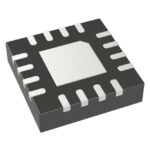 ADA4950-1YCPZ-R2
The activity of extra discounts on wholesale prices is in full swing…
Please fill in your contact information and we will send you the latest wholesale price list.