 ChipApex | Global Electronic Components Supplier
SEARCH
Search Product
Search Post
— IC芯片 | 连接器 | 传感器 | 被动器件 —
Search productSearch post
— IC芯片 | 连接器 | 传感器 | 被动器件 —
Consult the customer manager about the wholesale price.
consultation hotline:86-132-6715-2157
email:[email protected]
Contact the product manager for consultation. One-stop consultation is available.
Do you want a lower wholesale price? Please send us your inquiry and we will reply immediately.
The ADAU1328BSTZ is a high-performance, single-chip audio codec manufactured by Analog Devices Inc. It features two differential analog-to-digital converters (ADCs) and eight single-ended digital-to-analog converters (DACs). The device supports sample rates from 8 kHz to 192 kHz with 24-bit resolution. It operates on a single 3.3 V supply and includes an on-chip phase-locked loop (PLL) for clock generation. Key performance metrics include a dynamic range of 107 dB for ADCs and 108 dB for DACs, with a total harmonic distortion plus noise of -94 dB. The component is housed in a 48-lead LQFP package.
Verify the specific suffix BSTZ against the manufacturer's ordering guide to confirm the package type and temperature range. Confirm RoHS compliance status through official documentation. Check for end-of-life notifications or obsolescence warnings prior to finalizing procurement plans.
Select this component for applications requiring multi-channel output with differential stereo inputs. Ensure the design accommodates the 3.3 V supply requirement and provides adequate bypassing for AVDD and DVDD pins. Verify that the host processor supports the required SPI control port and serial data interface protocols.
This part belongs to the ADAU1328 family of audio codecs. Other members of this family may offer differential DAC outputs instead of single-ended configurations. The datasheet indicates availability in a 48-lead LQFP package for the single-ended output version.
Consult the manufacturer's current product selection guide for direct replacements or updated revisions. Verify pinout compatibility and electrical specifications if substituting with other members of the ADAU1328 family or newer generations.
The device features an on-chip PLL that can generate the master clock from the LR clock or an external crystal. It can also operate in direct master clock mode, eliminating the need for a separate high-frequency clock source.
For best performance, the ADCs should be driven from a differential signal source. Each input pin should be isolated using a series connected external 100 Ω resistor and a 1 nF capacitor to ground.
Yes, the internal voltage reference can be disabled via the PLL and Clock Control 1 Register. This allows the FILTR pin to be driven by an external source to scale the DAC output level.
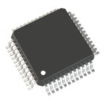 ADAU1328BSTZ
The activity of extra discounts on wholesale prices is in full swing…
Please fill in your contact information and we will send you the latest wholesale price list.





