 ChipApex | Global Electronic Components Supplier

SEARCH
Search Product
Search Post
— IC芯片 | 连接器 | 传感器 | 被动器件 —
Search productSearch post
— IC芯片 | 连接器 | 传感器 | 被动器件 —
Consult the customer manager about the wholesale price.
consultation hotline:86-132-6715-2157
email:[email protected]
Contact the product manager for consultation. One-stop consultation is available.
Do you want a lower wholesale price? Please send us your inquiry and we will reply immediately.
ADC09SJ1300AAVTQ1 is listed in the Analog To Digital Converters (ADC) range at ChipApex. The manufacturer field lists Texas Instruments. Its product description is IC ANALOG TO DIGITAL CONVERTER. Review the specifications below when checking this part for your BOM.
The ADC09SJ1300AAVTQ1 is a single-channel, 9-bit analog-to-digital converter (ADC) from Texas Instruments. It operates at a maximum sampling rate of 1.3 GSPS with a full-power input bandwidth of 6 GHz. The device features a differential full-scale input voltage of 800 mVPP-DIFF and utilizes an internal non-interleaved architecture. Performance specifications include a signal-to-noise ratio (SNR) of 53.5 dBFS and an effective number of bits (ENOB) of 8.5 bits at 100 MHz input frequency. Power consumption is rated at 940 mW when operating at 1 GSPS. The component is housed in a 144-ball FCBGA package.
Verify that the specific ordering suffix matches the required package type and temperature grade. Confirm that the AAV suffix corresponds to the 144-ball FCBGA package dimensions. Ensure compatibility with the intended system power supply voltages of 1.1 V and 1.9 V before finalizing procurement orders.
Select this model for applications requiring high-speed single-channel conversion with low power consumption. Verify that the 9-bit resolution meets the dynamic range requirements for the target signal. Ensure the host system can support the JESD204C interface protocols and provides adequate clocking infrastructure for the 1.3 GSPS operation.
This component belongs to the ADC09xJ1300-Q1 family, which includes quad and dual-channel variants. All members share the same 1.3 GSPS sampling rate, 9-bit resolution, and 6 GHz input bandwidth. The primary distinction lies in the channel count and the corresponding number of available JESD204C output lanes.
Direct replacements within the same family include the ADC09DJ1300-Q1 (dual-channel) and ADC09QJ1300-Q1 (quad-channel). These parts share identical electrical characteristics but differ in channel count and pinout configurations.
The maximum baud-rate supported by the JESD204C interface is 17.16 Gbps.
Yes, the device supports Subclass-1 mode for deterministic latency over the JESD204C interface.
The device features an optional internal phase-locked loop (PLL) with an integrated voltage-controlled oscillator (VCO) capable of generating frequencies between 7.2 GHz and 8.2 GHz.
Explore related parts through Data Acquisition, Integrated Circuits (ICs), all product categories, ChipApex homepage.
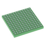 ADC09SJ1300AAVTQ1

The activity of extra discounts on wholesale prices is in full swing…
Please fill in your contact information and we will send you the latest wholesale price list.




